Thursday, December 15, 2005

Fiber Based Laser Tweezers & NSOM Probes

Little known is that most efforts in Fiber based NSOM, use optical fiber probes which are inherently lossy - in that dielectric optical guiding is lost between the tip and the optical waveguide over a relatively large "characteristic length" between the tip apex and the beginning of the undistorted optical core of the fiber optical waveguide.

As a consequence, the metal clad glass tip will absorb a fair bit of light and in collection mode little of the light collected from the tip will actually enter into the dielectric core, resulting in little collected light from a Betzig style probe will make it to the far end of the optical fiber due to cladding losses


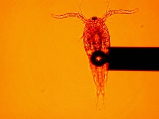
Fiber based laser tweezer gently gripping a mollusk ~0.4mm long


Most any Betzig style NSOM fiber probe used by most researchers in NSOM, will perform pretty miserably in optical collection mode, since the photons that enter the tip apex have a relatively low efficiency in making their way to the large enough diameter of the optical core that has not been distorted down to the tip diameter.

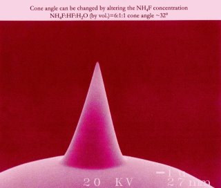
But there is a way to make 20nm sharp purely etched fiber probes, very consistently and with excellent collection efficiency.......

The same basic method of probe formation can also make a unique and superb optical fiber based laser tweezer, at much lower cost than a conventional far field focus spot laser tweezer...

PICTURES COURTESY OF ROD TAYLOR CNRC
( his works )
[click on pictures for larger views]


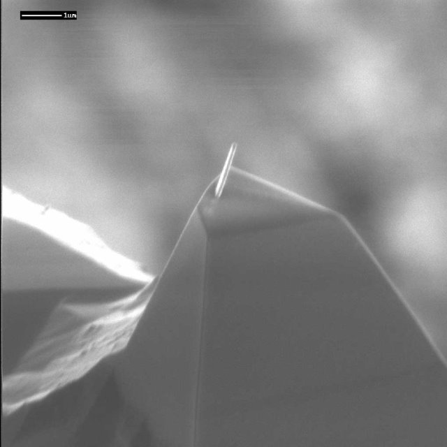
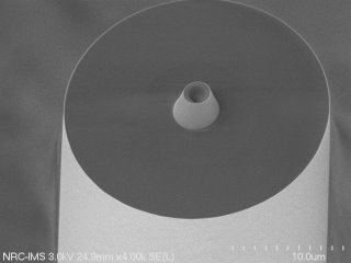
Sharp Tip Etched NSOM probe - note large optical core diameter at base of tip - critical for high optical collection efficiency in
NSOM.


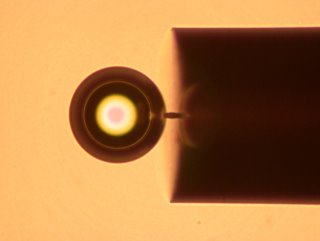
Fiber Tweezer Tip Detail - note divot in "tip" for Laser Tweezer
gripping cells - NOT FOR NSOM


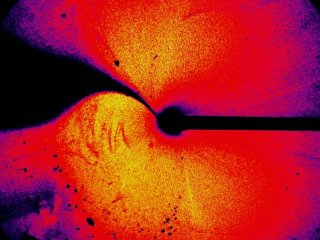
Fiber Laser Tweezer Trapped Bubble in Liquid


The helical vortice from laser tweezer liquid heating


POSTSCRIPT Feb 5th 2006


An unspoken area of application for high collection efficiency NSOM Probes is for optoelectronic circuit diagnostics of advanced MOS devices.

There is a fair bit of activity in high speed optoelectronic circuit diagnostics by imaging using microscopy and hot carrier photoemission for (sub?)ps timing analysis using conventional microscopy at Credence in Fremont and their purchased technology from a firm they bought called Optonics a few years back. Theirs is conventional microscope optics to a ?gated ?intensified cooled camera in ?IR

A fiber based method would possibly beat far field imaging hands down for RT circuit node data extraction BUT the issue will be since this is backside imaged ( requires substrate thinning on a BGA flip chip like P4/ Athlon 64 etc ) the backside thinning will likely limit the effective optical path length so that spatial localization is not optimal ( ie not truly near field, but likely to be far better than microscope lens collection to a camera ).

None the less, ps optical emission circuit diagnostics are astounding and this might be the first way to try to make an equivalent modest cost quasi nearfield "photonic oscilloscope probe" All this is conjecture on my part, but I would not be surprised based on prior efforts in mems based nanoscale circuit probing that we see an NSOM based photonic "oscilloscope" probe in the near future based on the excellent collection efficiencies available with this kind of low loss NSOM optical collection probe. I suspect someone is trying this RIGHT now....

Feb 14th 2006

Curious thought - can an effective combined NSOM, AFM and fiber based laser tweezers be implemented? Basically this comes down to whether sharp tip NSOM AFM can properly implement laser trapping with correct / optimal light wavelength and power, without appreciably degrading the other functions.

JOURNAL REFERENCES -
1) R.S. Taylor and C. Hnatovsky “Particle trapping in 3-D using a single fiber probe with an annular light distribution” Optics Express,11,2775-2782,2003.
2) R.S.Taylor and C. Hnatovsky “Trapping and mixing of particles in water using a microbubble attached to an NSOM fiber probe” Opt. Express 12, 916-928, 2004.
3) R.S. Taylor and C. Hnatovsky “Growth and decay dynamics of a stable microbubble produced at the end of a near-field scanning optical microscopy fiber probe” J. Appl. Phys.,95, 8444,2004.
4) P.Burgos,Z. Lu,A. Ianoul,C. Hnatovsky,M.-L. Viriot,L.J. Johnston and R.S. Taylor “Near-field scanning optical microscopy probes:a comparison of pulled and double-etched bent NSOM probes for fluorescence imaging of biological samples”,J. of Microscopy,211,Pt.1, 37-47,2003.
5) R.S. Taylor, K.E. Leopold, M. Wendman, G. Gurley and V. Elings, “Scanning Probe Optical Microscopy of Evanescent Fields”, Rev Sci. Inst., V69, Nr8 p2981
6) R.S. Taylor, K.E. Leopold, A. Delâge, M. Wendman, G. Gurley, V. Elings, "Near-field scanning optical microscopy", Physics in Canada 54 (2), 116-121 (1998).
7) R.S. Taylor, K.E. Leopold, M. Wendman, G. Gurley and V. Elings, "Bent-fiber near-field scanning optical microscopy probes for use with commercial atomic-force microscopes", Proc. SPIE V.3009, p. 119 (1997).


the Bibles - References for Microfabrication

Thin Film Processes by Vossen and Kern
( especially Ch 6 Wet Etchants table by Deckker and Kern )
BTL Silicon Technology
Handbook of Chemistry and Physics

Ed Graper's ( Lebow Inc / TFI Telemark )
Table of Thin Film Evaporation - materials and properties

Dan Flamm's text on Plasma and RIE Etching


Cadherins and Looming Revolution in Cancer Treatment ( Adherex )

A little known but critical technical advance in the treatment / shrinkage of solid tumors is currently in development by a very small but very talented firm that is the merger of a McGill university spinoff and a firm ( Oxiquant ) founded by more experienced cancer treatment physicians.

Adherex Technology, originally from McGill has been working on its methods for applying cell adhesion compounds to safe and selective destruction of tumor vasculature.

Where is the significance one might ask? Plenty and it is not "run of the mill me too"....

CLICK READ MORE... for rest of article.

A rare drug candidate that has exceptional tumor selectivity, fast acting 30 minute basic effect on the particular ( n-cadherin ) marked soft tissue tumors, and what appears to be no upper dose limit to onset of toxicity found ( the ADH-1 compound is normally made in small amounts by the body ), and the compound is safely metabolized quickly in 4 hours with no traces found therafter.

Susceptible n-cadherin marked tumors can exhibit onset of safe tumor necrosis in 30 minutes of the ADH-1 compound being administered.

Sorry there is little press on the firm, but this comes from the fact that in Canada most of the press online is by subscriber only and archives are accessable only for fee and not google indexed.

As a result, few know about this looming revolution in cancer therapy, that is going to take the world by storm in a few years as it progresses through FDA trials. ( currently completed Phase 1 and into Phase 1B / 2 concurrently ) Phase 1 showed both tumor shrinkage and no side effects what so ever )

Besides this novel ADH-1 chemistry, Adherex is also engaged in developing an improvement to the chemotherapy agent 5FU to increase the probability of being orally adminstered, and improve patient endpoints, and reduce side effects, after eyeing a failure in Glaxo's efforts to do the same, and seeing where they could remedy the percieved errors in prior implementations.

Key technologists include Adherex co-founder Prof. Orest Blaschuk of McGill Urology and Dr. William Peters, president of Adherex.

Watch for this one.

[ed - more of Adherex posts are linked just below]

adherex-phase-1-ADH-1_Combo-clinical-trial-announcement

adherex-receives-regulatory-approval-for-dosing-increase

article-on-genesis-of-adherex


http://finance.yahoo.com/q?s=ADH&d=t on AMEX and
http://finance.yahoo.com/q?s=AHX.TO&d=t on toronto


Trends in Scanning Probe / Atomic Force Microscopy

( NOTE - LIST IS IN NO PARTICULAR ORDER
Moreover if you are inexperienced in SPM the most critcal sauce in best in class instrumentation is

1] SOFTWARE - robustness of code, ease of re-programmability, nanolitho, # of useful features & max image pixel counts .... and
2] CONTROLLER HARDWARE - simplicity yet power through elegant feature rich designs.

There is only one firm with both of these criteria met in their core products.

The scanner and probe interests reflected in this post are somewhat avant garde - not yet reflected in commercial products, moreover with Degertekin's FIRAT, probe technology might soon become quite an interesting area as to innovation ...enuf said to the afficionados out there and there seem to many readers in the South Coast who know this obvious stuff well. ED. )

Faster imaging

Parallel probe microscopes commercialized


( picture - by kind permission of Prof. Cal Quate of Stanford )


Softer forces


Sharper and duller tips
( controlled radius )

R/T imaging - bio & materials, in air and fluid


Ando's fast bio scanner


Ando's Microscope Optical Detection Path


( pictures of Real-Time Scanning BioMolecular AFM - by kind permission of Prof. Toshio Ando, Kanazawa University )


Improved stability conducting nanoprobes


Higher pixel count imaging
( like the best 4th gen uScope controllers )

Lower tracking servo error excursions
( less force error - reduced under & overshoot excursions )

Methods for commercial nanotube modified tips of good orientation and yield


Prospects for Nanoimprint Lithography in IC fab

Aside from the obvious fact of the advantages of the Molecular Imprints technology for nanoimprint ( from UT Austin ), the primary limiter for possible success of nanoimprint litho in near mainstream IC fabrication, is in the mask fabrication infrastructure for the sub 50nm ( typical 30-40nm ) features to make the technology transition worthwhile for commercial manufacturers stuck with expensive working DUV technology.

Any effort to commercialize nanoimproint litho is critically dependent on customers ease of finding sources for the small feature 1x NIL masks in a timely fashion.

And the most difficult aspect to make the ultimate in small features in quartz is that most RIE processes and etchers, designed for use with conductive substrates, and needing to generate surface biases to critically assist in etching the SiO2 of the Quartz NIL mask, do not generate adequate surface potentials due to capacitive coupling through the 1/4" quartz....

A quandry - and what to do????

there has to be some kind of solution to this technical challenge ???

Wednesday, December 14, 2005

The Strategic Importance of DUV Immersion Lithography


picture of an unrelated relic of the beginnings of IC litho production


DUV immersion litho is potentially the engine of 65nm and smaller IC lithography with no exotic EUV xrays and no need for 157nm calcuim fluoride lens materials for the reduction lens. Onwards to immersion ..

update Feb 5th 2006
- or there might be some competition nm precision with stepped offset double exposures... rumors of this abound for the leading edge production litho, prior to rollout of immersion tools for production. Apparently Intel does not use immersion yet, and the 65nm process is actually producing 35nm wide physical gate lengths ??? HOW is the question, and double expose with precision stage offsets is one way to do this. A clue would be on the die's transistor layouts for min feature / smallest gate length devices to see all the gates oriented in the same direction for minimum CD transistors. That would be a clue that stepped offset 2x exposure might be used in the process to acheive minimum "sub-optical" CDs.....

update Feb 10th 2006
A well known leader of a famed reverse engineering firm in Ottawa, has practically confirmed the unidirectional orientation of MOS gate electrodes in the most advanced Intel devices. This so far anecdotal evidence, seems to support the possible implementation of nm scale precision, stepped offset dual exposure as a potential means to generate suboptical gate lengths at Intel - among other possiblities, and its success at delaying interest by Intel in immersion litho step and scan litho tool buys, apparently.

SMRs - Suspended Microfluidic Resonant sensors / detectors

Curious devices these are, using mems techniques to make suspended microfluidic channel resonators. These devices integrate a microfluidic biochemical / protein concentrator structure directly coupled to a MEMS suspended microfluidic channel - cantilever resonator, for mass balance detection of detected material.

Similar to a more conventional QCM - quartz crystal oscillator mass shift detection, but with the added twist of suitablity to biochemistry applications of wet chem detection - biomedical and biochemical.

Apparently the devices protoyped to date by Manalis' group in MIT have not yet yielded any (public) detection sensitivity advance over more conventional QCM mass balance detection - for reasons unknown.

A couple of thoughts I had relate to the sensitivity challenges -

CLICK READ MORE... for rest of article.

1] that pressurized microfluidic flows ( if pressurized from the coupled integrated fluidic biochemical concentrators ) might stiffen the suspended microchannel cantelevers in unpredictable ways, and

2] that the signal to noise of the sub 100Khz resonators might not be optimal - which if the present structures are retained, might gain benefit from the methods used in the more advanced recent design Inficon QCM thin film thickness rate controllers - by using a transmitted and received pulse train for the detection of the mass shift, rather than a quasistatic excitation.

Inficon's more novel QCM thin film thickness monitors, employ a patented method to send out a pulse train waveform near resonance, and cleanly detects a reflected pulse train (while not transmitting) to interrogate for phase and amplitude detection - with NO CW excitation of the QCM crystal.

In some sense this is very close to the techniques used in Acoustic microscopy - with some variation that the acoustic path length / time delay is nominally fixed in a sensor interogation, versus acoustic microscopy application.

Apparently Inficon's novel QCM signal methods have useful benefits to resolvable minimum detectable mass change in the Inficon thin film controller / monitor.

How this might be analogously implemented in SMRs of Manalis is something to think about, and as to whether the Inficon methods might benefit the S/N or detectable sensitivity of the novel SMR, and if it is possible to do at all.

Something to ponder.

UPDATE - Feb 3rd 2006
- come to think of it, if the SMR is operated discrete stopped flow, the pressure stiffening / desensitizing concern can be alleviated by stopped flow, and interleaved resonance interrrogation. By depressurizing the microchannel, any pressure stiffening can be eliminated as a sensitivity concern, although pressure decay relaxation time constant might slow the Quasi Real Time Performance. AHA !

Sunday, December 11, 2005

PDMS Microfluidic Mixer - Lateral Pneumatic Concept

12-11-05 At the same 12-8-05 Thursday Bay Area MEMS Journal Club Meeting, Narayan Sundararajan of Intel described in his presentation to the group, some interesting development work that Intel is persuing in the Digital Health R&D work. Fascinating stuff, microfluidics and single molecule detection methods and more.

Nara described several things that he has been working on, and there was emphasis on novel innovations - oriented towards building blocks for single moelcule detection with microfluidics.

There was description of a 3-d fluidic sheath confinement method which employs a lateral and more tricky vertical sheath flows to permit 2D confinement of a flowing analyte - to enchance S/N in flourescence detection of low concentration analyte flows and to avoid wall interactions by use of the flowing sheath protection.

Nara also talked about a unique simple to fabricate lateral pneumatic PDMS microfluidic actuator - that can rely on using only a single PDMS molded layer to implement pneumatically actuated fluidic mechanisms with a very simple microfab process. No complicated multi layer soft lithography required to build some pretty sophisticated devices. This was very innovative and Nara demonstrated a functioning peristalic pump implemented using the method, as well as a simpler variable flow restrictor.

Nara brought up the point that the smooth flat vertical sidewalls - in the thin membrane sidewall actuators - were not able to implement a lateral pneumatic actuated mixer. It was not stated so explicitly, but this was apparent from what was described in trying to observe mixing with the flat sidewall devices.

I saw this and had my interest piqued, since I remember that when fluid flows make sharp turns, the resultant lateral/radial gradient in flow velocity, generates a dispersive effect in the flow profile past the sharp turn.

Clearly this observation could result in a useful method to make a variation of the lateral pneumatic PDMS structure, to enable a multistage mixer for the channel flow, when surrounded by a PDMS lateral pneumatic structure. The sidewall shape just had to be modified to generate lateral flow velocity gradients.

When Nara said that the smooth sidewalls of the tested lateral PDMS pneumatic channel did not mix - the observation I had was to replace the smooth horizontal PDMS wall profile of the pneumatic actuator - with either a zig zag, or series of protrusions of some indeterminate shape periodicity and (a)symmetry ( 1 sided or 2 sides of the lateral pneumatic PDMS actuator )

So this is what we will attempt to prototype in the coming months to demonstrate that the simple cost effective lateral pnuematic PDMS channel actuator ( valve / peristaltic pump structure concepts ) might be extended to flow mixing with similar PDMS single layer process simplicity.

One of the challenges will be to ensure that the foot of the PDMS wall still adheres to the substrate to maintain a seal to the fluid channel, and the second will be to observe how the mixing efficiency varies with 1] the shapes of the tested sidewall lateral profile, 2] # of "mixing elements" and 3] asymmetry of the structures.

I remember several efforts at generating mixers in PDMS microfluidics and the challenges are not particularly trivial such as in DEP ( dielectrophoresis ) microfluidic mixers for example.....

Friday, December 09, 2005

NanoMetrology Improvement in Atomic Force Microscopy

12-09-2005 I will describe a novel method to improve nanoscale metrology using high aspect ratio scanning nanoprobes ( Atomic Force Microscopy )

Nanoscale metrology of very fine nano/ microfabricated features is extremely challenging. Accurate nanoscale metrology of structures formed in Integrated Circuit manufacture and development is important commercially.

Regrettably, Scanning Probe Microscopy metrology runs into what one might call an "probe artifact limited" resolution Barrier to metrology / imaging resolution of small "nanofabricated" structures, such as one finds in deep submicron Integrated Circuits and the like.

Seemingly desireable very high aspect ratio probe tips, bend flex and experience slip stick effects, which can limit usable metrology repeatablity and working "resolution" performance of the intended measurements. This occurs even with tapping mode imaging or other resonant imaging modes that are commonly associated with dramatic reductions in lateral / frictional slip stick.

The most troublesome of these artifacts arise from bending and flexing of extremely small and high aspect ratio probe tips as found with nanotube modified tips, electron beam deposited tips, or FIB - focused ion beam shaped / modified tips, where one has desirable high aspect ratio conceivably useful for imaging smaller high aspect ratio sample features, but the resultant images are often prone to undesireable step artifacts, limiting lateral dimensional metrology accuracy at the nanoscale.

This occurs even when resonant cantilever imaging modes such as Tapping ( RMS amplitude detection ) which already greatly reduces slip stick effects to a minimum, since nothing is dragging on the surface as with contact mode imaging.

CLICK READ MORE... for rest of article.

The interest in using nanotube modified like filametary like probe tips ( by modifying a more conventional microfabricated Atomic Force cantilever probe ) to attempt to scan / image / measure Integrated Circuit features often runs into a simple, yet challenging issue.

High aspect ratio "Filametary" extensions to the Apex of the probe tip, can be of usefully high aspect ratio and small enough diameter of tube/filament extension, to profile small structures such as sub 100nm wide gaps / vias / contact holes or similar.

BUT in using such a small filamentary nanotube like tip, the nanotube or other very high aspect ratio "filament" itself contributes substantially to image artifacts in the AFM image, due to the softness of the high aspect ratio slender nanotube ( or FIB shaped tip or electron beam depositied nanotip for examples), even when using resonant cantilever imaging modes.

If the end of the contacting tip moves laterally in a significant variable manner, relative to the probe cantilever body or larger conventional tip base, it can get a bit challenging to acheive desireable nanoscale accuracy in the measurement one is trying to undertake.

AFM microscopes controllably scan an XY image field pattern or some derivative ( like the predictive/adaptive scanning fields ) to form an "image data 2 D extent" not necessarily rectangular or square, but more often than not conventional 2D image XY scan field - rectangular or square.

The Z or height data of the sample being imaged, is most typically derived from constant force data obtained by servoing the probe cantilever for constant bend / force while scanning in 2 dimensions the lateral image extents.

( sample surface tracking can be done with contact mode, tapping or ostensibly "non-contact" / FM detection resonant modes - but the concept is basically the same - constant force servoing whether it be with RMS amplitude detection or phase / Frequency servoing ). Tapping type imaging tends to be preferred, with non-contact resonant imaging a useful alterative as both modes are largely free of simpler frictional lateral streaking type artifacts ( slip stick ).

One can produce constant height data from the Scanning Probe measurement and likewise lateral metrology of features with height defining edges setting the feature widths to be measured ( taking into account the ideal rigid body assumption of the probe tip shape ).
This is often called CD or critical dimension measurement in the terminology of IC fabrication.

It is often wrongly thought that this softness of the nanotube modified AFM tip, makes the potential application of nanotube modified tips nearly worthless for accurate lateral metrology, due to the buckling and bending the of the tube - mounted or grown at the probe tip apex, may experience.

But if one closely examines the actual behaviour of the slender nanotube while imaging, some key points become observable ( with a resonant cantilever probe imaging mode ).

Over relatively flat surfaces, few artifacts due to bending or buckling can be observed if the scan speed is kept to usefully low speeds - and the lateral bending can be made fairly consistent hence able to be "calibrated for" or compensated for in accurate metrology.

And obviously the probe force ( amplitude / force constant ) needs to be kept reasonably low to mitigate excessive buckling of the high aspect probe region, while scanning on relatively flat surfaces.

Usefully low forces can be obtained by lower resonance amplitudes for tapping imaging, or by using probe cantilevers of low enough force constant or combinations thereof.

Nanoscale metrology is often related to measurements of widths of fabricated structure lines ( eg. MOSFET gates, wiring interconnect for a few common examples ) or etched holes, as is found in fabricating electrical vias before interconnect wiring deposition as another interesting metrology example...observed in commercial IC fabrication.

These structures to be measured are NOT flat and do cause noticeable metrology error term artifacts when imaging with a nanotube or other high aspect ratio probe ( even seen with an FIB - focused ion beam shaped / modified probe tip, if the aspect ratio of the FIB filament tip is high enough / soft enough in lateral force constant )

Careful observation of the probe tip behavior while scanning, by understanding the image artifacts present when traversing noticeable step height topography, will see that much of the undesireable seemingly tricky behaviour of the slender high aspect ratio nanotube tip is mostly compression buckling of the nanotube when the probe is descending a step.

In contrast to the errors due to descending related buckling of the slender region of the high aspect ratio tip, when the nanotube or other slender filament is Ascending or climbing a step - the tube / filament is under TENSION and as such has pretty usefully accurate step placement needed for accurate lateral dimensional metrology.

Regrettably most all imaging control and analysis programs for Scanning Probe Microscopy (nano) metrology, do not provide any useful program code or routines to do the obvious improvement - reconstruct a synthesized image for metrology applications - of step edge position, where the image data is comprised mostly of relatively flat regions and steps.

How can a more accurate synthetic image of of AFM data using a nanotube or other high aspect ratio tip, be derived from artifact laden images that have tubes experiencing compressive buckling placement errors on descents of steps, be calculated?

Since Atomic / Scanning Probe Microscopes move the AFM probe tip cantilever typically in a raster pattern - with Trace and retrace ( as called in DI / Veeco Nanoscope instruments for example ), the probe goes back and forth across the mostly similar region at least 1 full cycle back and forth ( with slight offset in the slow scan direction between trace and retrace line data).

In traversing what we will call here the Forward Direction, most all features with have 1 side having the probe ascending ( rising ) in that "image" line data set, and the nanotube / high aspect ratio tip will be under tension on the rising edge of the step, with attendent benefits to the accuracy of the metrology of the rising step lateral placement ( low bending buckling tip artifacts ).

And the other step side of typical features ( still with the tip moving in what we are calling the "Forward scan direction" ), will have the probe tip descending "other" step, with the result that the "descending" features which the nanotube / high aspect ratio probe tip will likely experience noticable buckling related lateral errors, with somewhat random tip "placement" - very undesireable for accurate lateral nanoscale dimensional metrology.

We can generate data that is a subset of line data from each of two fast scan directions - to derive a data set which the nanotube / high aspect ratio tip is either quasi static ( nearly neutral / slight compression, or in tension), ie free of major tube/ tip related compressive buckling data errors, with the tip ascending larger steps, reconstructed by an data image line pair or two directions of scanning mostly over the same physical region, using rising tip data or flat regions taken selectively from the two opposite direction line data sets..

One determines from the first direction's data set, the compressively artifacted buckling ( descending tip ) regions - and replaces these error prone data subregions, selectively with the same physical region scanned in the opposite direction. The probe tip will have now scanned that previously descending step, in the opposite direction, by ascending the same step, eliminating or greatly reducing the magnitude of compressive buckling lateral error artifacts of the high aspect region of the modified AFM tip.

This method of scan data synthesis permits algorthmic elimination of major step descending buckling error artifacts from reducing metrology accuracy of lateral dimensions.

There are variants of the proposed method that can be applied to adaptive scanning for faster metrology data aquisition that are apparent from this innovation.

There are technical details of issue here - the opposite direction data sets have to be sufficiently well calibrated in correlation of physical data points to be of practical use. In one type of instrument this is partially accomplished with a variety of calibration constants in the scan calibration.

But the implementation of the required algorithm to derive a scan data set that is proincipally free of larger compressive buckling artifacts from a slender flexible probe descending a step is fairly straightforward to do.

One can easily envision that this can also be applied to novel scan fields - non-orthogonal and efficient scan field subsets that implement tracking scan fields and the like.

There is the possibility of applying this method of derived image data, mostly free of compressive probe tip buckling artifacts in rotated image scan fields and when the typical box averaging algorithms are employed for addressing the minor metrology error term seen with unaveraged data, where line roughness is not desired to be a contributor to the measurement (error ) of a feature width.


Enter your email address:

Delivered by FeedBurner

Subscribe to Wendmans Views on Nanotech by Email