The Strategic Importance of DUV Immersion Lithography
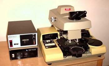
picture of an unrelated relic of the beginnings of IC litho production
DUV immersion litho is potentially the engine of 65nm and smaller IC lithography with no exotic EUV xrays and no need for 157nm calcuim fluoride lens materials for the reduction lens. Onwards to immersion ..
update Feb 5th 2006
- or there might be some competition nm precision with stepped offset double exposures... rumors of this abound for the leading edge production litho, prior to rollout of immersion tools for production. Apparently Intel does not use immersion yet, and the 65nm process is actually producing 35nm wide physical gate lengths ??? HOW is the question, and double expose with precision stage offsets is one way to do this. A clue would be on the die's transistor layouts for min feature / smallest gate length devices to see all the gates oriented in the same direction for minimum CD transistors. That would be a clue that stepped offset 2x exposure might be used in the process to acheive minimum "sub-optical" CDs.....
update Feb 10th 2006
A well known leader of a famed reverse engineering firm in Ottawa, has practically confirmed the unidirectional orientation of MOS gate electrodes in the most advanced Intel devices. This so far anecdotal evidence, seems to support the possible implementation of nm scale precision, stepped offset dual exposure as a potential means to generate suboptical gate lengths at Intel - among other possiblities, and its success at delaying interest by Intel in immersion litho step and scan litho tool buys, apparently.
mw


0 Comments:
Post a Comment
<< Home