 1 Click Subscribe to the RSS feed
Giessibl's AFM Atomic Force Microscopy with Astounding Subatomic Imaging Resolution
 A brilliant scientist, Prof. Giessibl now at Uni Regensburg in Germany, has both industrial experience at Park Scientific Instruments ( the early Stanford spinoff in AFM ) and collaborations with Sr. IBM Zurich researchers in state of the art imaging.
Part of Giessibl's notable advance in my interpretation, was a seemingly simple but key observation that prior efforts to use quartz crystal tuning forks as tip resonators for AFM, all suffered from phase noise in resonance from asymmetric vibrations of the two tines of the resonator, when the quartz tuning fork was used as a force sensor in non contact Atomic Force Microscopy.
This is because the sensor was operated in AFM applications with unbalanced dynamic forces - unequal between the conventional two vibrating tines one with the mounted nanoprobe and the 2nd unloaded (redundant) free tine.
The phase noise is easly reduced by operating the sensor as a single clamped tine (quartz arm) and a single vibrating tine - merely by gluing one of the quartz tines to a fixed support.
The oscillator structure still works, but the resonance is no longer asymetric when used as an AFM force sensor, and now the shift in phase or frequency of the oscillator due to the probe forces are now more closely correlated to the actual forces exerted on the probe / single vibrating tine.
Aside from this keen insight and very novel innovation, Prof. Giessibl predicted theoretically that this would have material improvements on the ultimate performance of Atomic Force Microscope imaging resolution. His astounding accomplishment was to take the ultimate resolution of AFM imaging into uncharted waters for AFM imaging performance, typically assumed to be only the purvey of STM Scanning Tunneling Microscopy - Subatomic imaging resolution.
Aside from this improvement in resonator function for NC AFM, Giessibl has a novel means to cleave silicon wafers? to make near atomic probe tips - which the technique no doubt is a fine art. And a highly refined understanding of Non Contact AFM probe forces.
 The refined UHV AFM instrument where the astounding image results were produced.
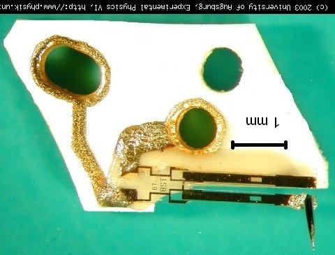
The novel sensor of Prof. Giessibl's minds eye - that enables Atomic Force Microscopy at Sub Atomic Resolution.
Note that the quartz tuning fork glued to the alumina substrate is harvested from a SWATCH or other inexpensive quartz watch, by carefully cutting open the resonator can and gently removing the etched and patterned conventional quartz resonator. Observe that the upper tine (arm) is glued to the substrate. The importance of this gluing or fixing of the upper non sensing tine is described below. This gluing is a critical but simple innovation that Franz determined essential by careful modeling and observation, with the consequence of enabling subatomic resolution in AFM imaging - a long time holy grail acheived 1st by Prof. Giessibl, and long thought only possibly with STM tunneling microscopy.
STM tunneling microscopy requires conductive sample materials, while AFM can image conducting and insulating material equally well.
HIGH RESOLUTION AFM IMAGING RESULTS
look at higher image resolution versions by clicking on the respective pictures below
( all images with kind permission of Prof. Franz Giessibl )
look at higher image resolution versions by clicking on the respective pictures below
( all images with kind permission of Prof. Franz Giessibl )
| AFM-Image with 77 pm resolution | |
 | AFM-Image with 77 pm (picometer) resolution. Subatomic structures are visible within single tungsten atoms. Image size 500 × 500 pm2. |
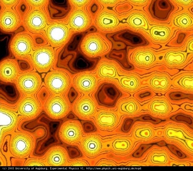
| Revealing the hidden graphite-atom | |
 | Revealing the hidden atom in graphite with AFM showing all atoms within the hexagonal graphite unit cells. Image size 2×2 nm2. |
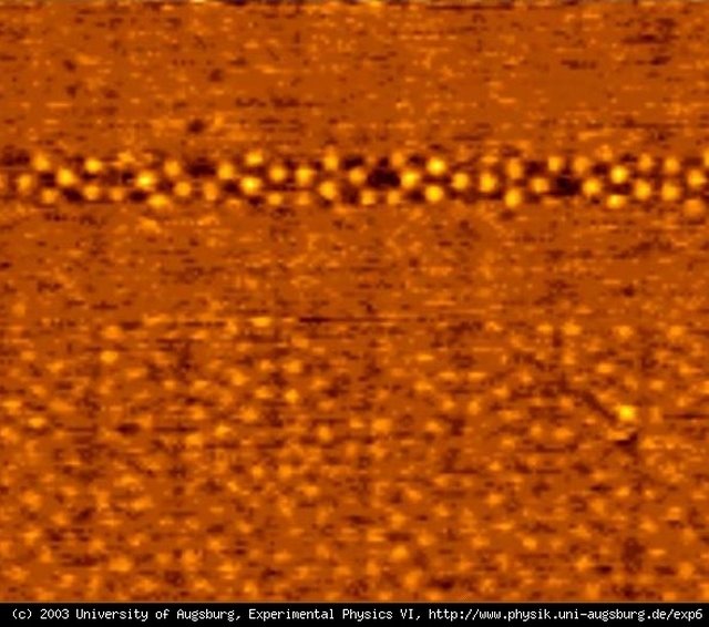
| AFM image showing steps on a Si (111) surface | |
 | Steps on (111) orientated silicon wafer imaged with a Nanosurf easyScan DFM. Advanced Lab Course 20, Augsburg University, EKM, Experimentalphysik 6. |
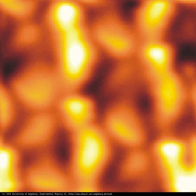
| STM image of silicon, obtained with a lateral force sensor | |
 | Image of a Si surface imaged with a lateral force sensor. In the left half of the image, the cantilever does not oscillate, in the right half it oscillates with an amplitude of 0.09 nm, yielding a double image of every atom. |
| AFM image of silicon, obtained with a qPlus force sensor with a single crystal silicon tip | |
 | AFM image of silicon, obtained with a qPlus force sensor with a single crystal silicon tip. Image size 3.3 nm x 3.3 nm. [Ann. Phys. (Leipzig) 10, 887 (2001)]. |
| Subatomic resolution by atomic force microscopy Gerhard Richter Erster Blick | |
 | First experimental image showing internal atomic structures [Science 289, 422 (2000)]. This image has inspired Gerhard Richter, one of the most influental contemporary painters, to craft the lithographic print "Erster Blick" (2000). See: Dietmar Elger, "Gerhard Richter: Biografie und Werk", Dumont, Cologne 2002, pp 119-120. |
| Subatomic resolution by AFM | |
 | First experimental image showing internal atomic structures. Note the crescent shaped feature inside the silicon? atoms. (click on pic for enlarged detailed image) |
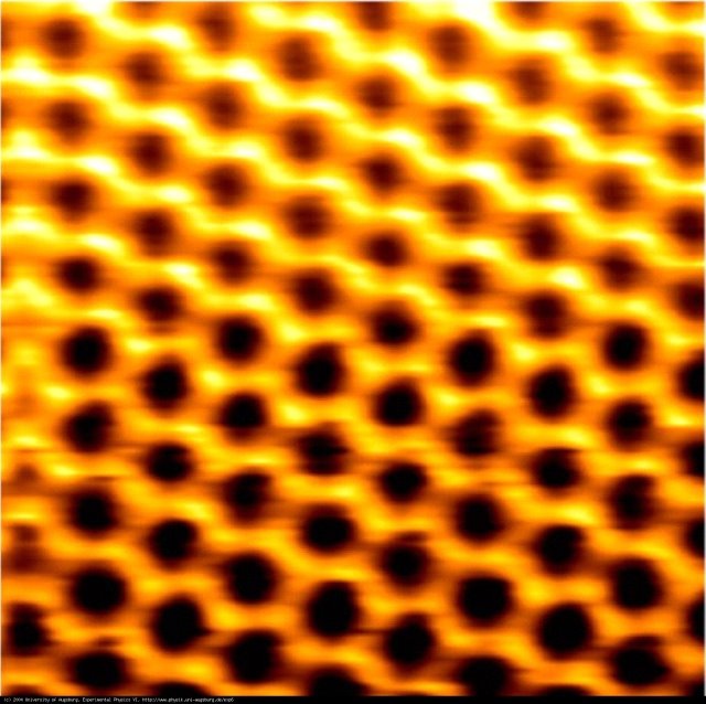
| First atomic resolution AFM image of a reactive surface Silicon Si (111) - (7x7) | |
 | First atomic resolution AFM image of a reactive surface. Image size 18 nm x 18 nm. Science 267, 68 (1995). |
wendmannanotechnologynanonanotech
scanning+probe+microscopemicroscope+near+field
microscope+atomic+forcemicroscope+afm
microscope+stmmicroscope+tunnelingafm+hansma
quateelingselings+digital+instruments
elings+veeconanosensorsnanoprobe
posted by Mark Wendman at 2:01 PM
![]()
![]()


1 Comments:
Hi Mark,
This is Matt from Semiconductor Insights.
Just a quick note to introduce you to our new blog SemiSerious. Judging from your blog, and that you link to our company (!), you may find it good reading.
http://www.semiconductorblog.com
I would appreciate any comments or criticism you may have.
Thanks,
Matt
Post a Comment
<< Home