 1 Click Subscribe to the RSS feed
Novelx Silicon Micromachined Electron Microscope
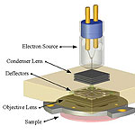
Novelx is a relatively new startup emerging into early productization of their SEM based on innovative compact Silicon Micromachined Electron Optics. The microscope is considerably smaller footprint than a typical scanning electron microscope, and has an excellent miniaturized Field Emission electron source and well designed electron optics.

The firm was founded by two talented industry veterans, Drs. Lawrence Murray and James Spallas with over 20 years of combined experience in miniaturized SEM columns starting back at IBM in 1990 and continuing on at Applied Materials ETEC division subsequently. Both are highly skilled in the microfabrication of specialized electron optics and design of same.
From their website.....
Novelx has miniaturized and driven the cost out of the core technology inside conventional Scanning Electron Microscopes (SEMs) to create a disruptive innovation. Our patented Silicon Stack Technology™ enables Novelx to build the Nano E-beam Engines™ that will drive innovation in a variety of nanotechnology applications including:
* Imaging - the viewing of nano-scale objects,
* Metrology - the measurement of nano-scale materials and features,
* Lithography - the writing of nano-scale features directly on substrates.
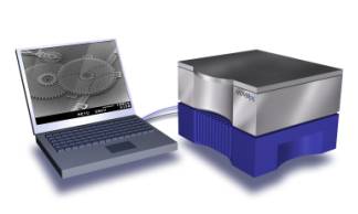
Novelx's first product is the mySEM™, a nano-scale imaging system that provides those at the cutting edge of discovery and innovation with low-voltage, high-resolution images of nano-scale objects. In the form factor of a desktop printer and connecting directly to a laptop computer, the mySEM is a breakthrough product technology. Novelx believes that seeing innovation drives discovery. Contact us directly to learn more about our products.
Powered by the Novelx Nano E-beam Engine, the mySEM electron microscope delivers nano-scale imaging capabilities directly to the desktops of individuals creating the next generation of innovations in nanotechnology. The mySEM is a breakthrough technology that is affordable while providing outstanding price performance in a compact design with an intuitive user interface. As easy to maintain as it is to use, the patent pending e-beam cartridge design ensures that your images are always the best they can be while avoiding expensive and unnecessary maintenance.
Here are 2 issued patents of Novelx as of Jan 2008.
I have not as yet read through these, but there is some prior art in stacked layers in micromachined SEMs / electron optical columns, that it is curious if this was referenced in these patents?
| 7109486 | Layered electron beam column and method of use thereof An electron beam column package comprises a plurality of layers having components, such as lenses, coupled thereto. The layers may be made of LTCC, HTCC or other layer technology. |
| 7045794 | Stacked lens structure and method of use thereof for preventing electrical breakdown A micro-electrical system, such as a lens stack for use in a scanning electron microscope, analysis tool, etc., comprises recesses and/or serrations that increase the surface path breakdown, thereb... |
wendman nanotechnology nano nanotech SEM Electron+Microscope Silicon+Micromachining MEMS IBM ETEC Applied Materials Electron+Beam+Lithography Maskless Lithography KLA Tencor Veeco Intel 65nm nanometrology ebeam lithography
posted by Mark Wendman at 2:52 PM
![]()
![]()


0 Comments:
Post a Comment
<< Home