 1 Click Subscribe to the RSS feed
TETRAD of PhotoVoltaic Materials Strategies for the future
Things to Ponder
SILICON - variations on process & module methodology
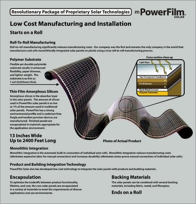
single xtal, thin film and poly xtal, hot wire cvd and small chips, Prof. Sach's edge fed string growth, emerging/ speculative silicon nanowire and the superb engineering of Sunpower's sophisticated devices......and now a large scale 13" wide - roll to roll amorphous silicon on polymide flex at Iowa Thin Film Technologies AKA Powerfilm Solar
the cast of millions goes on and on...
CONT'D - click READ MORE.... for the full scoop.
POLYMER Photovoltaics -
Konarka
The best top flight VCs are betting on this.
The most prestigous board and advisory team.
1] founding scientists
2] industry advisors
3] science advisors
Based on names alone it will likely succeed.
And very notably, Prof. Heegers superbly prolific patenting is beyond merely impressive, an astounding personal ~60 career patents.
Kudos to Prof. Heeger !
Will a means be found to inhibit UV / environmental degradation needed for a competitive product life ?
Will it be possible to coax stable and usefully high PV efficiency from some as unknown EVIDENT materials solution? ( silly pun of mine )
Feb 14th Konarka announces another $20m funding round completed lead by 3i ventures, making a total $60m raised since 2001.
Stay Tuned .... ( again a silly pun only a photon would love ? )
NANOCRYSTAL PV conversion
Nanosys - seems to still be struggling with %PV conversion efficiency
as Konarka seems to be ?
Are tetrapods all they are cracked up to be?
Cyrium Technologies - Fafard's Nanoscale Self Assembled EPI Quantum Dot solar cells
Simon F. says he can hit in excess of 40% conversion efficiciency for space based cells, the real question is whether he will get bit by the bug for larger price sensitive markets and try to put some effort into a scalable production worthy terrestrial oriented PV device based on SA Quantum Epi Dots. Fafard is CNRCs quantum dot expert, and spent time in a post doc at UCSB under the ever fascinating and mercurial Pierre Petroff.
Cyrium does need to increase the size of the patent portfolio that is certain, as the firm is nowhere near the # of filings of larger competitors, but likely is that Cyrium's present funding is a notable constraint. Simon's core IP is represented in "Solar cell with epitaxially grown quantum dot material" United States Application 20050155641, which describes successively cascaded tuned QD PV elements merely grown epitaxially.
For now that is all that is apparent in the relevant IP posted at USPTO. If it makes it to an issued patent, this might be of considerable value, beyond the bond layer transfer tandem cells being studied at Caltech and elsewhere, merely on ease of manufacture, by avoiding the multiple bond layer transfer of this earlier innovation practiced at the Atwater Lab.
Technically at some point, the self evident paradigm to try, is to leverage the methods fairly recently implemented at Motorola for III-V low defect EPI growth on large silicon wafers, for his devices.
Question is whether Cyrium has motivation, interest or knowledge for how to do so. If yes to all 3, and one can acheive comparably high efficiencies on larger wafers from "mere" epi growth, question is, will this catalyze a larger terrestrial market and higher profits, when competing against for example SunPower's lean mean manufacturing machine? "Only a photon knows for sure ..."
Thin Film CIGS
Miasole Promising but capital intensive ( almost unnecessarily so with the advanced custom magnetron sputtering cathode that was entirely unnecessary to be part of the complex critical path in the production process development - despite the appeal of high utilization cathodes, where was it impotant in determining the actual panel / module process flow - NOWHERE ??? and costly thin stainless substrates.
And it is likely that they made 2 Process strategy ERRORS. The stainless flex substrates have a host of implied problems - mostly related to singulation and possible edge shorting of the cell structure during singulation, not to mention adhesion / CTE mismatch issues in the thermal cycling for CIGS interdiffusion activation.
The described method of shear cutting the edge of the web steel, while it looks clean in cartoon pics, is risking serious damage to the junction integrity of the CIGs stack, unless a laser preclean is done to remove the CIGS stack from proximity to the sheared edge - but with still yet the remaining risk of shear induced cracking of CIGS in proximity to even a cleaned edge of the stainless substrate.
Furthermore laser processing of materials on top of stainless flex substrate is going to make the laser process window considerably smaller than desired due to high power losses to the steel (heat sinking), which is completely undesireable for a good industrial (yag) laser ablation process. And yes athermal fast excimer pulses will help, but at much greater cost than typical industrial grade YAG laser thermalized processing. And if you still yet need more process window - the trick will be to reduce the laser power required with reactive gas assist laser etching rather than purely ablation, while it may make a useful process window, will result in consdierably higher capital costs, nevermind some risk to the CIGS itself. So high thermal conductivity ( steel) substrates for web fed CIGS are coming with some considerable baggage technically.
Therefore, while steel has an obvious ( to those who have workd with laser ablation process ) serious set of disadvantages in process integration, the potential aesthetic and relaibility appeal is quickly lost in practice.
The means to slightly shift things in ones favor, is to carefully examine process windows and adapt materials to
and naturally in module integration is the ever present, tantalizing yet slightly fickle ....
Roll To Roll Processing
Nanosolar ( PV ink ) as a Paradigm for cost reduction for module formation and further mention to the "ROLL MASTERS" large scale 13" wide - roll to roll amorphous silicon on polymide flex at Iowa Thin Film Technologies AKA Powerfilm Solar
Roll to Roll has unique materials and structure requirements to acheive long life cells, and forces the manufacturer to look closely to find capable production equipment for end to end Roll to Roll.
RtoR sputtering is easy to procure std equipment for, but patterning / ? screen printing takes a bit more effort ) [ come to think of it - screen printing or resist litho & etch in RtoR, is almost silly - just go with Shadow Masked metal sputtering for the coarse PV interconnect features - with no need to etch, nor fire a screen printed paste ]
and more speculatively - will the Vitex Barix process find a home in environmental barriers in some of the more novel PV advances ( as it has been successful in OLED stabilization without the use of hermetic sealed packages ). This is something only an OLED pioneer might know?
musings to follow later .......
wendman solar+power solar+energy solar+panels solar+cells photovoltaic nanosys Sunpower konarka Cyrium Nanosolar Miasole powerfilm DFJ NEA Jurvetson Heeger Alivisatos
quantum+dot quantum+dot+solar+cells nano nanotech nanotechnology global+warming renewable+energy clean+tech
SILICON - variations on process & module methodology
single xtal, thin film and poly xtal, hot wire cvd and small chips, Prof. Sach's edge fed string growth, emerging/ speculative silicon nanowire and the superb engineering of Sunpower's sophisticated devices......and now a large scale 13" wide - roll to roll amorphous silicon on polymide flex at Iowa Thin Film Technologies AKA Powerfilm Solar
the cast of millions goes on and on...
CONT'D - click READ MORE.... for the full scoop.
POLYMER Photovoltaics -
Konarka
The best top flight VCs are betting on this.
The most prestigous board and advisory team.
1] founding scientists
2] industry advisors
3] science advisors
Based on names alone it will likely succeed.
And very notably, Prof. Heegers superbly prolific patenting is beyond merely impressive, an astounding personal ~60 career patents.
Kudos to Prof. Heeger !
Will a means be found to inhibit UV / environmental degradation needed for a competitive product life ?
Will it be possible to coax stable and usefully high PV efficiency from some as unknown EVIDENT materials solution? ( silly pun of mine )
Feb 14th Konarka announces another $20m funding round completed lead by 3i ventures, making a total $60m raised since 2001.
Stay Tuned .... ( again a silly pun only a photon would love ? )
NANOCRYSTAL PV conversion
Nanosys - seems to still be struggling with %PV conversion efficiency
as Konarka seems to be ?
Are tetrapods all they are cracked up to be?
Cyrium Technologies - Fafard's Nanoscale Self Assembled EPI Quantum Dot solar cells
Simon F. says he can hit in excess of 40% conversion efficiciency for space based cells, the real question is whether he will get bit by the bug for larger price sensitive markets and try to put some effort into a scalable production worthy terrestrial oriented PV device based on SA Quantum Epi Dots. Fafard is CNRCs quantum dot expert, and spent time in a post doc at UCSB under the ever fascinating and mercurial Pierre Petroff.
Cyrium does need to increase the size of the patent portfolio that is certain, as the firm is nowhere near the # of filings of larger competitors, but likely is that Cyrium's present funding is a notable constraint. Simon's core IP is represented in "Solar cell with epitaxially grown quantum dot material" United States Application 20050155641, which describes successively cascaded tuned QD PV elements merely grown epitaxially.
For now that is all that is apparent in the relevant IP posted at USPTO. If it makes it to an issued patent, this might be of considerable value, beyond the bond layer transfer tandem cells being studied at Caltech and elsewhere, merely on ease of manufacture, by avoiding the multiple bond layer transfer of this earlier innovation practiced at the Atwater Lab.
Technically at some point, the self evident paradigm to try, is to leverage the methods fairly recently implemented at Motorola for III-V low defect EPI growth on large silicon wafers, for his devices.
Question is whether Cyrium has motivation, interest or knowledge for how to do so. If yes to all 3, and one can acheive comparably high efficiencies on larger wafers from "mere" epi growth, question is, will this catalyze a larger terrestrial market and higher profits, when competing against for example SunPower's lean mean manufacturing machine? "Only a photon knows for sure ..."
Thin Film CIGS
Miasole Promising but capital intensive ( almost unnecessarily so with the advanced custom magnetron sputtering cathode that was entirely unnecessary to be part of the complex critical path in the production process development - despite the appeal of high utilization cathodes, where was it impotant in determining the actual panel / module process flow - NOWHERE ??? and costly thin stainless substrates.
And it is likely that they made 2 Process strategy ERRORS. The stainless flex substrates have a host of implied problems - mostly related to singulation and possible edge shorting of the cell structure during singulation, not to mention adhesion / CTE mismatch issues in the thermal cycling for CIGS interdiffusion activation.
The described method of shear cutting the edge of the web steel, while it looks clean in cartoon pics, is risking serious damage to the junction integrity of the CIGs stack, unless a laser preclean is done to remove the CIGS stack from proximity to the sheared edge - but with still yet the remaining risk of shear induced cracking of CIGS in proximity to even a cleaned edge of the stainless substrate.
Furthermore laser processing of materials on top of stainless flex substrate is going to make the laser process window considerably smaller than desired due to high power losses to the steel (heat sinking), which is completely undesireable for a good industrial (yag) laser ablation process. And yes athermal fast excimer pulses will help, but at much greater cost than typical industrial grade YAG laser thermalized processing. And if you still yet need more process window - the trick will be to reduce the laser power required with reactive gas assist laser etching rather than purely ablation, while it may make a useful process window, will result in consdierably higher capital costs, nevermind some risk to the CIGS itself. So high thermal conductivity ( steel) substrates for web fed CIGS are coming with some considerable baggage technically.
Therefore, while steel has an obvious ( to those who have workd with laser ablation process ) serious set of disadvantages in process integration, the potential aesthetic and relaibility appeal is quickly lost in practice.
The means to slightly shift things in ones favor, is to carefully examine process windows and adapt materials to
and naturally in module integration is the ever present, tantalizing yet slightly fickle ....
Roll To Roll Processing
Nanosolar ( PV ink ) as a Paradigm for cost reduction for module formation and further mention to the "ROLL MASTERS" large scale 13" wide - roll to roll amorphous silicon on polymide flex at Iowa Thin Film Technologies AKA Powerfilm Solar

Roll to Roll has unique materials and structure requirements to acheive long life cells, and forces the manufacturer to look closely to find capable production equipment for end to end Roll to Roll.
RtoR sputtering is easy to procure std equipment for, but patterning / ? screen printing takes a bit more effort ) [ come to think of it - screen printing or resist litho & etch in RtoR, is almost silly - just go with Shadow Masked metal sputtering for the coarse PV interconnect features - with no need to etch, nor fire a screen printed paste ]
and more speculatively - will the Vitex Barix process find a home in environmental barriers in some of the more novel PV advances ( as it has been successful in OLED stabilization without the use of hermetic sealed packages ). This is something only an OLED pioneer might know?
musings to follow later .......
wendman solar+power solar+energy solar+panels solar+cells photovoltaic nanosys Sunpower konarka Cyrium Nanosolar Miasole powerfilm DFJ NEA Jurvetson Heeger Alivisatos
quantum+dot quantum+dot+solar+cells nano nanotech nanotechnology global+warming renewable+energy clean+tech
posted by Mark Wendman at 5:22 PM
![]()
![]()


0 Comments:
Post a Comment
<< Home