Wednesday, March 29, 2006

Adherex Receives Regulatory Approval For P2 Dosing Schedule Increase

Adherex has received regulatory clearance from Health Canada to increase the dosing schedule of its Phase II study of single agent ADH-1 to once every week, from the previous dosing once every three weeks.

Adherex is also adding clinical test sites in the US. The ADH-1 clinical trial is presently being performed at six centers in Canada.

"Based on our experience from our North American and European centers, this more dose dense, weekly dosing schedule of ADH-1 has been well tolerated and is preferable from a pharmacology standpoint," said William P. Peters, M.D., Ph.D., Chairman and CEO of Adherex.

This P2 single-agent testing is designed to evaluate the anti-tumor activity and tolerability of repeated doses of ADH-1 in patients with lung, esophageal, adrenocortical, renal and hepatocellular cancers whose tumors express the molecular target N-cadherin.

The trial is now expected to enroll up to an aggregate of 100 patients.

Adherex expects the Phase 2 trial to complete in the second half of 2006.

more than enough to ponder the possibilities.........

[ed - more of my Adherex posts are linked just below]

adherex-phase-1-ADH-1_Combo-clinical-trial-announcement

article-on-genesis-of-adherex

cadherins-and-looming-revolution-in-cancer-treatment


Thursday, March 23, 2006

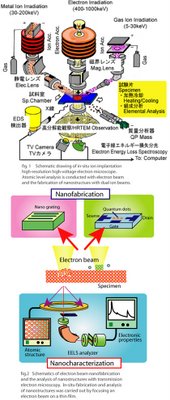
Japans NIMS Tsukuba nano materials lab group links

Nano Bio Device
Nano Device 1st sub group
Nano Device 2nd sub group
Nano Quantum Electronics
Atomic Electronics
Nano Synthesis and Engineering

Optoelectronic Nanomaterials

Electro Nano Characterization
Nano Synthesis and Analysis

Nano Characterization
Nano Function 2nd sub group
Nano Fabrication
Nano Function 1st sub group
Nano Function 2nd sub group
Nano Architecture
Nano Materials Assembly 1st sub group
Nano Materials Assembly 2nd sub group

Nano Materials Assembly 3rd sub group

Bio Nano Materials Group
Nano Quantum Transport
Extreme Field Nano Functionality
Nano Physics 1st sub group
Nano Physics 2nd sub group
Nano Physics 3rd sub group
Appointed Project Leader nano patterned media
Nano Quantum Foundry

NIMS Hybrid TEM dual ion beam FIB

Japan's NIM - National Institute for Materials - is Amazing

This Japanese National lab's Nanomaterials research web site is astounding.

Covers everything soup to nuts in just about anything nano materials related of substance. (I'll point out that those getting RSS feeds on PDAs might need a PC to get past the flash front page.) Most NIMS labs 10+? seem to have the requisite Scanning Probe Microscope. Each and every group has a narrow enough project focus complemented by notable bench depth of staff to persue their work with vigor.

There is enough description of each groups work to get a good understanding of the their respective emphasis of the research work.

I will be reading more from their pages in the coming weeks and will post interesting highlights.

From the quick glance I have taken, it reminds me of what Bell Labs used to be, but with the focus on anything and everything in nanomaterials - where the real action is in nano today.

As to more trendy nano PR - this has NONE - the research is ALL meat and potatoes.

VERY IMPRESSIVE.

Tuesday, March 21, 2006

Curious about relative importance of parasitic resistance in polymer and solution dispensed nanoparticle PV cells

I keep thinking over how it might be possible to raise % efficiencies in polymer or nanocrystal liquid dispensed PV cells. I spoke with a close friend of mine, a Carleton University EE alumni, who is very skilled in semiconductor physics. I am of more modest skill in semiconductor physics (esp. at a quantum level) but often times I see what others seem to miss in process / device technology.

He brought up the salient point that any nanocrystal embedded in a weakly conducting (polymer) semiconductor will inherently be at a significant disadvantage as compared to more conventional monolithic grown or pulled semiconductor PV cells, largely due huge increases in parasitic cell resistances, - active material to semiconducting PV resistances on a nanoscale and poor bulk contact resistances to polymer conductors / semiconductors.

Same goes for a dense conglomerate of nanoparticles being of higher contact and bulk resistivity than a solid of similar materials.

My short conclusion in the interim is that several noted efforts seem to be technically weak mostly due to an "achilles heel" of parasitic resistances being excessively high.

His and my interpretation re desires to improve conversion efficiencies based on the nanoscale convertors alone, is that this possibly misplaced focus will miss the key point that the resistances are seemingly overwhelming as key issues, and not per se the convertors themselves ( at a nanoscale ).

While much protestation to the contrary is implicit due to the recent scientific coverage focusing on the nanoparticle convertor materials, by several well and even superbly credentialled folks, I have some doubts as to the merits being claimed.

It is clear that Quantum Dots ARE important, but the systems level cell materials issues ARE important - even equally and possibly more so. IE you can innovate in the Qdots and miss on the cell nano/microscale integration (ohmic losses in particular).

Cyrium's quick work with superb conversion results is a strong data point in support of my argument - they have done fantastic nanoparticle based PV conversion engineering and have by merits of the monolithic EPI growth, no high parasitic resistance issues common to Nanosys and Konarka - by Cyrium's best in in class materials choices...

And yes Cyrium's cells will not be able to be made roll to roll, nor on polymer, nor overall lowest in cell growth costs / area, in the foreseeable future, due to the issues related to EPI growth, but 39% conversion efficiency is nothing to sneeze at.

Can someone even come close in overall coversion efficiency by solution based nanoparticle / polymer PV convertors? Quite a stretch for now and possibly far into the future. Not impossible, but not likely yet.

Can Evident's wavelength convertors quantum efficiency, surmount the polymer / solution dispensed nanoparticle resistance issues? I have a degree of skepticism about that, until there are unusual huge breakthroughs in doping and conductances of polymer PV materials.

I may well be wrong, but I'd love to hear explanations why?

I also see one possible avenue to circumvent these challenges of parasitic resistance, but the process / materials issues implicit, are neither non-trivial nor without costs (ie how much closer can one get to Cryium's benchmark % eff, versus the cost increases in processing by some speculative means?)

The specific analogies one might infer, are that both Konarka and Nanosys's efforts which focus on the basic nanoscale particle convertor materials, in the hope that efficiencies will improve with careful but so far speculative experiment, might be missing the boat re the fact that fundamentally, conducting polymers (excluding metal particle doped "poly-mets" for obvious host matrix reasons) and especially semiconducting polymers, do not seem to be able to be produced with low resistivities in the range of the typical 0.5 ohm-cm seen in best in class silicon cells (nor approach the low contact resistivities of silicon or CS pv cells either).

Or do I have my figures wrong here - esp re semiconducting resistivities and with good low ?ms range carrier lifetimes?

I am curious as to readers' thoughts on relative importance of nanoparticle intrinsic photoconversion quantum efficiencies versus the "nanoscale through microscale" resistive losses? PLEASE SEND / POST COMMENTS ...

This may well be a significant and possibly fundamental stumbling block to advances in solution processed nanocrystal type photovoltaic cells and polymer matrix hosted alternative photovoltaic convertors.

I'd hazard a guess that due to the properties of CIGS materials, this does not apply to NanoSolar's roll fed nanoparticle CIGS process. Despite the CIGS particle suspensions used as precursors, the material appears to have already high conversion efficiencies, and I'd tend to partially attribute this to CIGS low material resistivities versus the more avant gard polymer or semiconducting nanoparticle cell technologies.

Monday, March 20, 2006

Solaicx - Photovoltaic Silicon Crystal Mavens


Pullers / Growers and Slicers of single crystal silicon Par Extraordinaire !

This hardy battle tested crew is doing useful commercial improvements to both the CZ puller and thin wafer slicing to reduce costs of high mobility single crystal silicon wafers with high volumetric utilization of boule silicon and improved process uptime for the crystal puller.

Key in their IP from a silicon crystal puller expert of the name Bender(an inventor for the firm), is that they have devised a means to stabilize the CZ puller with a near continuous feed replenishment of the melt, without disturbing the melt interface (nor displacing the surface) and identified useful methods to enable thinner wafer slicing for high yield production, by mechanically stabilizing the wafer and and saw blade.

Seemingly mundane technology, but important for thin wafer production desired for lower costs in high performance solar cell manufacture. ( ie if you are going to do high performance high volume cost effective cells, it has to be single crystal silicon for the foreseeable future - as Sunpower among others, seem to know well)


Cyrium's 39% efficient Monolithic Quantum Dot Solar Cells

Novelx Silicon Micromachined Electron Microscope


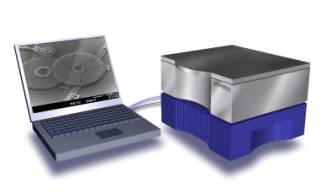
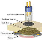
Novelx is a relatively new startup emerging into early productization of their SEM based on innovative compact Silicon Micromachined Electron Optics. The microscope is considerably smaller footprint than a typical scanning electron microscope, and has an excellent miniaturized Field Emission electron source and well designed electron optics.

The firm was founded by two talented industry veterans, Drs. Lawrence Murray and James Spallas with over 20 years of combined experience in miniaturized SEM columns starting back at IBM in 1990 and continuing on at Applied Materials ETEC division subsequently. Both are highly skilled in the microfabrication of specialized electron optics and design of same.

From their website.....

Novelx has miniaturized and driven the cost out of the core technology inside conventional Scanning Electron Microscopes (SEMs) to create a disruptive innovation. Our patented Silicon Stack Technology™ enables Novelx to build the Nano E-beam Engines™ that will drive innovation in a variety of nanotechnology applications including:

* Imaging - the viewing of nano-scale objects,
* Metrology - the measurement of nano-scale materials and features,
* Lithography - the writing of nano-scale features directly on substrates.


Novelx's first product is the mySEM™, a nano-scale imaging system that provides those at the cutting edge of discovery and innovation with low-voltage, high-resolution images of nano-scale objects. In the form factor of a desktop printer and connecting directly to a laptop computer, the mySEM is a breakthrough product technology. Novelx believes that seeing innovation drives discovery. Contact us directly to learn more about our products.


Powered by the Novelx Nano E-beam Engine, the mySEM electron microscope delivers nano-scale imaging capabilities directly to the desktops of individuals creating the next generation of innovations in nanotechnology. The mySEM is a breakthrough technology that is affordable while providing outstanding price performance in a compact design with an intuitive user interface. As easy to maintain as it is to use, the patent pending e-beam cartridge design ensures that your images are always the best they can be while avoiding expensive and unnecessary maintenance.

Here are 2 issued patents of Novelx as of Jan 2008.

I have not as yet read through these, but there is some prior art in stacked layers in micromachined SEMs / electron optical columns, that it is curious if this was referenced in these patents?

7109486 Layered electron beam column and method of use thereof
An electron beam column package comprises a plurality of layers having components, such as lenses, coupled thereto. The layers may be made of LTCC, HTCC or other layer technology.
7045794 Stacked lens structure and method of use thereof for preventing electrical breakdown
A micro-electrical system, such as a lens stack for use in a scanning electron microscope, analysis tool, etc., comprises recesses and/or serrations that increase the surface path breakdown, thereb...


Sunday, March 19, 2006

CBC's Chasing the Cancer Answer - Wendy Mesley

CBC - Canadian Broadcasting Corporation posted an excellent series on Cancer called Chasing the Cancer Answers on March 5th 2006. Notable are the questions asked about prevention and the business of cancer. While the press more commonly obsesses about prospects for cures by new technology, this series is more down to earth in focus on possible causes and other interesting dynamics.

Here are the direct links to the articles

Chasing the cancer answer
Is cancer in our blood?
How blaming the patient is easier than prevention
The big business of cancer drugs and treatments
Consumer tips: Carcinogens to watch for
Key cancer questions in the chase for answers
Series Credits

And for a hint at how a major advance in cancer treatment is coming in the next few years - see these prior posts of mine on ADHEREX Technology, a spin off of McGill University. Adherex is a firm developing a novel cadherin (cell adhesion) based cancer treatment using their ADH-1 pharma compound.

Safe, effective, and fast acting in melting a portion of soft tissue tumor blood vessels (of tumors that have the n-cadherin marker), that appear to not be treated by conventional chemo.

In combo with conventional Chemo, ADH-1 holds unusual promise to lick cancer dead where thought impossible. Early preclincal combo tests, aside from advances in more typical tumors, demonstrated unusual promise against the otherwise untreateable melanoma.

My personal recommendation is that anyone having real challenges in the battle with cancer, consider enrolling in the upcoming combo therapy trials of Adherex's ADH-1. Contact the firm for more info, as of Jan 2007 this is in planning stages.

cadherins-and-looming-revolution

article-on-genesis-of-adherex


Friday, March 10, 2006

Belcher Lab (cambrios tech mostly) BaISA related pub titles Bio Assisted Inorganic Self Assembly

2005
Biomaterials functionalization using a novel peptide that selectively binds to a conducting polymer
Biological scaffolds for the peptide directed assembly of nanoscale materials and devices

2004

Bacterial Biosynthesis of Cadmium Sulfide Nanocrystals
A method for coupled transcription and aminoacylation of cysteinyl-tRNA
Virus-based genetic toolkit for the directed synthesis of magnetic and semiconducting nanowires
Layer-by-layer surface modification and patterned electrostatic deposition of quantum dots
Development of a novel method for surface modification of synthetic polymer using combinatorial peptide screening technologies
Biological Routes to Metal Alloy Ferromagnetic Nanostructures
Fabricating novel biomimetic polymers using combinatorial peptide screening technologies
Virus-Based Fabrication of Micro- and Nanofibers Using Electrospinning
Molecular orientation of a ZnS-nanocrystal-modified M13 virus on a silicon substrate
Virus-based toolkit for the directed synthesis of magnetic and semiconducting nanowires
Genetically Driven Assembly of Nanorings Based on the M13 Virus


2003

Viruses as vehicles for growth, organization and assembly of materials
Optical anisotropy in individual CdS quantum dot ensembles
Synthesis and organization of nanoscale II-VI semiconductor materials using evolved peptide specificity and viral capsid assembly
Building Quantum Dots into solids with well-defined shapes
Viral assembly of oriented quantum dot nanowires
Virus-based alignment of inorganic, organic, and biological nanosized materials
Optical spectroscopy of silicon nanowires
Spectroscopy of individual silicon nanowires

2002
Making new hybrid bio electronic and magnetic materials based on nature's design
Structural and microstructural characterization of the growth lines and prismatic microarchitecture in red abalone shell and the microstructures of abalone "flat pearls"
Emulating biology: building nanostructures from the bottom up
Ordering of quantum dots using genetically engineered viruses

2001
Biomolecular recognition and control of nano magnetic and semiconductor materials

2000
Protein components and inorganic structure in shell nacre
Borrowing ideas from nature: peptide-specific binding to gallium arsenide
Selection of peptides with semiconductor binding specificity for directed nanocrystal assembly

Tuesday, March 07, 2006

AkuBio's Resonance Acoustic Profiler - vs Manalis' SMRs


So now there is a practical implementation of a microfluidic Quartz Crystal Monitor - QCM?

Despite all the effort and money into MITs Manalis' Suspended Microfluidic Resonant Detectors - SMRs, Akubio a spin off from the UK Cambridge University, founded by Prof David Klenerman, is simple straightforward microfluidic channel, coupled to what appears to be a conventional quartz crystal oscillator.

Product seems to be up and running and developing real applications rather than focusing on the microscale fabrication / integration, like Manalis is doing with costly co-development with IMT MEMS of Santa Barbara, of intricate complex micromachined MEMS cantilever SMR microfluidic structures.

All in all, the method of coupling fluidic channels to detection / excitation oscillators is useful for studying chemical and biological effects / interactions. But rather than initially focusing on the MEMS as Manalis is doing, Klenerman's Akubio Technology is doing the right thing, which is focussing on the applications.

Yes one could do all kinds of handwaving that the real emphasis should be on making a small disposable in MEMS, but anyone with a good business sense would agree that critical is applications development for real uses, and a MEMS centric effort will not have enough effort placed on developing critical value added end use applications.

Right out of the chute, here are 3 classes of APPLICATIONS AkuBio is supporting in Life Science Research -

Protein Characterization
Resonant Acoustic Profiling enables the real time label-free analysis of molecular interaction kinetics and affinities by measuring the change in frequency and resistance occurring on an oscillating quartz resonator due to surface binding events. Here we outline the basic principles of this powerful detection technique and review the key steps of analysis.

Antibody Concentration & Antigen Cross-Reactivity
A number of methods are currently available for measurement of antibody concentrations, including colorimetric assays (ELISA, Biuret, BCA, Bradford), densitometric methods, and amino acid analysis. Unfortunately a variety of limitations associated with these techniques (long analysis times, lack of binding specificity, label interference), makes their use in certain situations non-ideal.

Resonant Acoustic Profiling technology overcomes these issues by directly measuring the specific binding of antibodies to target proteins. The assays are label free, rapid, and can be designed to measure only active protein binding. Here we present protocols for the determination of antibody concentrations and characterization of antigen cross-reactivity.

Affinity and Kinetic Characterization
Resonant Acoustic Profiling enables the real time label-free analysis of interaction kinetics and affinities for molecular binding partners. Here we present a method for the accurate measurement of the affinity and kinetics of the interaction between the small human protein myoglobin, which is widely used as a cardiac biomarker, and its corresponding monoclonal antibody.
..........................................

Sounds like a sensible start to a technology, which later after sufficient applications development, will then warrant focus on microfabricated integration, but hardly at the start is the cost and effort for complex microfabricated cantilevered microfluidics worth the effort. The end use focus has to come first - to be market driven so as to avoid more costly errors.

END OF POST

Enter your email address:

Delivered by FeedBurner

Subscribe to Wendmans Views on Nanotech by Email