Tuesday, February 28, 2006

Konarka's probable Austrian development arm

this research unit at the Uni Linz in Austria seems to have connections to Konarka. It has a wonderful list of online publications, dissertations and annual reports.

LIOS - Linz Institute for Organic Solar Cells

LIOS Publications


and online video lectures by Prof. Heeger on polymer electronics

Excellent reading and insight into one probable strategy of Konarka's development.

Wednesday, February 22, 2006

Compact Photonic Integrated Optical Circuits - Hybrid PhC Conventional Waveguides

One aspect to photonic crystal research that puzzles me greatly, is why it is commonly (wrongly) thought that PhC's should even be contemplated for general waveguiding use in integrated planar optical waveguides.

PhC's are nothing more than an extension of the concepts found in conventional thin film multilayer filter mirrors, but to the 2nd / 3rd Dimension. What is trivially evident in waveguiding applications, is that the nature of the granularity of micro/ nanofabricated PhC's is such that it is intrinsically "rough", filled with scatterers, as one might call it (apparent when one has critically trying to smooth the roughness of more common planar integrated optical dielectric waveguides for ultimate in low loss optical waveguide transport).

So it is unclear how PhCs might have benefits for general waveguide transport in integrated optics - since at first glance the basis for the structures - appears more like a scatterer than one might want to contemplate for use in optical waveguiding. And scattering from waveguide edges, results in lossy waveguide optical transport. This is not to disparage use of PhCs as integrated optical elements (as discrete integrated optical components in an integrated optical circuit), but it would seem intuitively that PhCs might have little promise as more general optical waveguiding transport elements.

I had the pleasure of working for an innovative professor at University of Alabama - who was very strong in computation of EM first principal effects in dielectric optical waveguides and PhC's.

Prof. Greg Nordin, who had the very sensible idea to do away with PhC's in the straight and simpler low bend radius optical waveguide sections, so as to reduce overall WG losses !!!

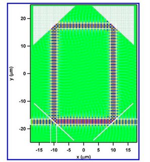
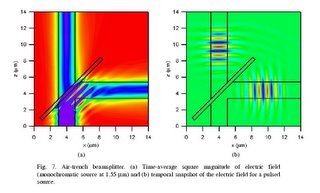
But still use PhC's novel capabilities in turning, filtering, splitting - for very compact integrated optical elements. Love it.

Prof. Nordin, now at BYU, is a perfect gentleman - smart as a whip and with profound insight into integrated optics and computational modeling of waveguide structure properties. He understands the proper use of novel structures in integrated optics and is an active researcher in design and computation of Photonic Crystal structures.

He has profound interest in small bend integrated optical structures - Air gap turning mirrors and optical ring like resonators and similar, made of air gap mirrors, both in modelling and nanofabrication.

CONT'D - click READ MORE.... for the full scoop.


Tuesday, February 21, 2006

Who was this Famously Accomplished Computer Designer


1] Who is this most accomplished CPU designer,
SEYMOUR CRAY

2] How many computer firms did he take part in, ( and the cities where he did his work )
SPERRY /UNIVAC, CDC - Control Data, Cray Research and Cray Computer - 4, mostly minneapolis, Chippewa Falls WI, and Colorado Springs Colorado

3] What was he most famous for in a particular feature of his hallmark computer architecture, -
Vector Floating Point Arithmetic units - SIMD - Single Instruction Multiple Data (the basic element to early supercomputing)

4] What unusual method did he have of CPU design methodology, -
circuit designs were written up as boolean equations both for custom ICs and for each circuit card in the computer, and field engineers never had classic schematics - just pin assigments to the boolean logics descriptions of computer cards

5] What were the sad tragic circumstances of his unfortunate passing.
He was killed in a triple rollover of his Jeep Cherokee when hit by a drunk driver crossing headon into his lane in Colorado. The Jeep Cherokee he was driving had as standard for this vehicle no support for the roof that could sustain a rollover force (nor any custom rollbars). The roof was crushed and he sustained brain damage contributing to his death from the crash. Absolute tragedy of monumental proportions.


Sunday, February 19, 2006

EPOCAL's Medical Lab Diagnostics on an active Microfluidic Smart Card


POSTSCRIPT 8-22-2015 / preamble > This post is attracting some modest revived attention, particularly by one anonymous reader, in part since I linked this in some few comments I made at Business Insider, about purported technical novelty of Theranos' microfluidic lab tests.

The technology behind both Epocal and Theranos' microfluidic blood tests likely has some generic similarities particularly in function and miniaturization, despite each having gained patents.

Notable if not key, is that in the microfluidics and Micro Total Analysis fields going back to the early 90s, there is a massive hord of patents granted since Dr. Jed Harrison and others in Europe ( Andreas Mainz ) started the field called uTAS micro total analysis. Many of the patents are overlapping in function, albeit different specifics of miniaturization. Meaning many of the patents in this field applicable to miniaturized medical diagnostics are of imperfect intellectual property FTO Freedom To Operate, or do not block others from similar function / miniaturization by different specifics in implementation.

What is clearly unique about Theranos and full credit to the team, is not per se the use of microfluidics in blood medical diagnostics (described in their early patents onwards), but their market go to strategy, to go after conventional blood lab services, via retail outlets, and with microfluidic diagnostics and small blood samples combined, and notably to have developed apparently 400 or more blood tests and counting implemented on their microfluidics platforms.

Again huge credit to Theranos and Elizabeth Holmes, but the core ( microfluidics enabled aspects ) of their technology still is not as unique as some imply ( and do not describe publicly except in Theranos' "public patent documents" )

As to the claimed $8 Billion valuation of Theranos, there are aspects to this that are debateable. Given apparently 400 microfluidic miniaturized clinical grade blood tests have been developed, the "valuation" of the firm is far higher than Epocals when Epocal was sold to Inverness Biomedical ( Boston and San Diego ) just a few years ago, where Epocal apparently had very few tests finished development on its also unique microfluidic blood test platform.

But given that mature incumbents in conventional Blood Lab testing have valuations in the range of Theranos's present value, and serve 1,000 or more ( poss 2,000) types of blood tests albeit with mostly conventional venous blood draws presently, I'd guess Theranos gains some value over conventional incumbents, but not as much as one might hope, just yet ( meaning the $8B valuation claimed due to private equity invenstment valuations might be slightly inflated, not by much ) as the incumbents if getting their act together might not have huge difficulty in mounting competitive microfluidic lower cost blood test offerings at retail pharmacies, to compete against Theranos.

Theranos's patent portfolio functional blocking strength might not be as strong as hoped for due to the plethora of microfluidic uTAS patents, and just for example Epocal's core technology, presently not deployed yet outside of hospital clinical bedside settings, but easily used / modified for pharmacy small blood volume collection for regional Epocal type microfluidc blood testing or actual in Pharmacy tests with similar apparatus.

To be fair, Theranos has a huge jump - early competitive advantage in large scale pharmacy collected microfluidic blood tests. Full credit to the team, market and sales and product strategy can matter more than core technology in company valuations.

But even the earliest dates of patents from Epocal and Theranos are comparable dating to 2005 / 2006 ( of microfluidic topics - hardly comprehensive coverage then )

While the recently recurring anonymous reader might have issues regarding the Canadian aspect to Epocal ( why I do not know ) Epocal was bought out by an American firm in the last 5 yrs, exactly when I do not remember. Inverness Biomedical (now called ALERE) a large firm in Boston and San Diego owns Epocal.

back to the original post dating to 2006 _______________________________________________
Epocal, based in Ottawa Canada, a microfluidics health care diagnostics firm founded by Dr. Imants Lauks, is building a novel compact microfluidics blood diagnostics analyzer on a card, for wide deployment in health care facilities.

Dr. Lauks previously was the founder of i-Stat, later acquired by Abbott, whose biochip based products provide hand held solutions for a number of critical care assays, including: Blood Gases, Electrolytes, Chemistries, Coagulation, Hematology, and Cardiac Markers (cTnI).

Epocal is noteworthy for its vertically integrating microfluidics process / manufacturing capability, with medical chemistry applications expertise.

Where the i-Stat's devices seemed to be mostly passive dedicated substrate sample chips, the Epocal solutions will be lab on a card ( smart card format with integrated active microfluidics, sensors and reagents ) deployed to be measured and logged on small Epocal card readers in the hospital floor setting.

No muss nor fuss - all the wetted parts - channels and sensors and pumps, are on the disposable cost effective smart cards.

Noteworthy is the development at Epocal of smart microfluidic card manufacturing on flex - ie roll to roll substrates. And leveraging the considerable infrastructure / industrial tooling of smart card manufacturing.

This - use of mostly industry standardized smart card manufacturing tooling - is rare for recent attempts to commercialize biotech microfludics diagnostics, especially noteworthy for being readily available off the shelf from numerous vendors.

Epocals Biosensors-on-Flex™ technology processes kapton flex circuits into biosensor arrays in a single continuous roll to roll manufacturing process.

Epocal uses Roll to Roll processing - from raw material manufacturing start, all the way through to finished diagnostic card ready for shipment and use, with rapid throughput in manufacturing.

Roll to Roll Flex circuits are processed using machinery modifed from standard smart card manufacturing, on standard tape-on-reel tooling

Epocal's smart flex substrate cards integrate all active and passive microfluidics to eliminate the need for external pumps, detectors, reagent cartridges etc.

This is a practical manufacturable commercial implementation of micro TAS - Total Analysis System, with a large targetted focused market - hospital blood chemistry tests - test results faster and cheaper than ever before.

The flex kapton based smart card module, forming microfluidics with through vias and back-side metal, is the platform for a generalized biosensor micro Total Analysis system. Each card film via through hole pocket, when loaded with membrane or chemical reagent, implements a microscale bioreactor with integral electrochemical detector.

Membranes and reagents are loaded by roll to roll process integrated micro-dispensing onto the 35mm tape carrier, resulting in the lowest cost solution of any integrated biosensor technology.

Epocal has developed membranes and reagents for application in blood tests that include electrolytes, dissolved gases, hematocrit, and metabolites. Epocal's initial product will be capable of 8 tests, later expandable to12 tests per card.

My take is this firm will be another blockbuster from Dr. Lauks - comparable but likely better than i-Stat became.
Epocal Inc.
2319 St. Laurent Boulevard, Suite 500
Ottawa Ontario K1G 4J8 Canada
Phone: 613-738-6192 Fax: 613-738-6195

recent news from Epocal
Epocal Inc. Completes $31 Million Series C Financing 4/11/2007
Epocal Inc. Receives FDA Approval To Market The EPOCTM Blood Analysis System 0/12/2006

................................................
MW - postscript Sept 2007 -

Below are some pictures explaining the function of the Epocal microfluidics
smart cards, unique for being early in clinical diagnostics deployment, with the high functional complexity on the plastic card, supported by the readers and data management system. Click on them to see higher resolution images.


Here are the published patent and patent applications at USPTO of Epocal at the moment.

US20070170062 INTEGRATED ELECTROKINETIC DEVICES AND METHODS OF MANUFACTURE
Devices with electrokinetic elements are disclosed as well as their method of microfabrication for use in micro-scale analysis, mixture separation and reaction. The devices consist of solid hydrophilic-matrix films that have been microfa...
7214300 Integrated electrokinetic devices and methods of manufacture
Devices with electrokinetic elements are disclosed as well as their method of microfabrication for use in micro-scale analysis, mixture separation and reaction. The devices consist of solid hydrophilic-matrix films that have been microfa...
7201833 Integrated solid-phase hydrophilic matrix circuits and micro-arrays
The invention is directed to analytical devices and micro-arrays with integral fluidic inputs and outputs. The devices are constructed from planar solid-phase hydrophilic matrix circuits containing dry chemical reagents overlaying integr...
7094330 Heterogeneous membrane electrodes
The present invention relates to planar electrochemical sensors with membrane coatings used to perform chemical analyses. The object of this invention is to provide unit-use disposable sensors of very simple and economical construction, ...
US20050150761 Electrode module
A chip-carrier module known from smart card technology is adapted as an electrode array for use in disposable sensing or separation devices containing electrodes. The electrodes are manufactured directly onto chip-carrier module. The pre...
6896778 Electrode module
Planar devices incorporating electrodes for performing chemical analyses are disclosed. The devices include an electrode module in a fluidic housing. The electrode module includes a carrier module and at least one electrode thereon. More...
6845327 Point-of-care in-vitro blood analysis system
Devices for cost-effectively performing in-vitro diagnostic chemical analyses at multiple distributed locations within a medical institution are disclosed. One object of this invention is to provide a network of distributed sensory devic...

And here are issued patents at the Canadian Patent Office (CIPO)

CIPO - Patent - 2449388 INTEGRATED ELECTROKINETIC DEVICES AND METHODS OF MANUFACTURE


CIPO - Patent - 2547701 INTEGRATED SOLID-PHASE HYDROPHILIC MATRIX CIRCUITS AND MICRO-ARRAYS


CIPO - Patent - 2449511 POINT-OF-CARE IN-VITRO BLOOD ANALYSIS SYSTEM


CIPO - Patent - 2449172 PLANAR ELECTRODE MODULE FOR USE IN A DIAGNOSTIC DEVICE

CIPO - Patent - 2547698 POTENTIOMETRIC REFERENCE ELECTRODE WITH HETEROGENEOUS MEMBRANE


.........................................


Watch for Epocal.....

Saturday, February 18, 2006

Intel's Superb IC Manufacturing - the Best Bar None

hmm.. How many ways can one wax poetic upon the best in the business?

Intel's technical discipline, expertise, visionary technology developer, and overall well managed business is well known, but often misunderstood in the true depth of the astounding diversity of strengths.

CONT'D - click READ MORE.... for the full scoop.

Despite minor ups and downs (no-one escapes this), Intel has an astounding track record in developing and manufacturing the worlds most advanced Integrated Ciruit microdevices of unprecedented density and speed, at unparalleled manufacturing volumes. Bar None.

While scientists are impressed by raw technology, notable is that Intel is not merely among the best, if not the best microfabrication technology development team in the world, but can turn visions of the future into tangible reality, on a manufacturing scale no other firm in the IC industry can replicate in the slightest. And never stop at drive to improve performance on a scale others cannot come close to.

Intel's list of worlds firsts in novel technology, starts long ago with the now forgotten 1103 nMOS Dram memory - a 256 bit memory built on 2 inch silicon wafers.

A little known fact about the then revolutionary 1103, is that this 1st MOS memory device was the key to the revolution in GUI Personal Computers - it was the system memory device used in the Xerox PARC Alto graphical interface computer, the conceptual foundation of the personal computing paradigm in use today.

The seeds of Intel's success were found in the tenacity of Intel's team in the days of the 1103 - a take no prisoners approach to process problem solving, to make the promise of dense MOS digital devices a tangible commercial reality, beyond visions in theoretical papers. The struggle for yield in the early days of this key device was indeed a struggle and a test of team character.

There was one person who made all the difference in the 1103's early yield improvement - persisting in the face of challenges, and all kinds of pressures. He knows who he is, a modest, friendly and unassuming fellow who put the critical yield improvement brick into place that let the 1103 find its success. The future astounding commercial success of MOS IC technology followed, with the proof of the 1103's market storm, revolutionizing both dense computer memory technology and computers themselves.

Aside from the 1st commercially successful MOS devices, the 1st microprocessor, and the first EPROM (electrically programmable ROM) there are a multitude of device and product technology firsts, born from this unquestioned leader of the industry.

The evolution of MOS technology has largely been driven by Intel's vision and drive to suceed, focused, persistent, and relentless in intent. And may they keep at it, into the age of Nano now upon us, with all the success due the firm and its hardworking, astoundingly talented employees and management team.


Thursday, February 16, 2006

On the Delay / Cash Needs of Solar Cell Startups Miasole and Others

re SiliconBeat's 2/15 post on Solar Power Startups Taking More Cash & Time

hmm... well this gets interesting. Most anything BUT silicon for solar cells comes with all kinds of baggage - higher costs, more complex (and even speculative) chemistry, real risks in RESEARCH that properly are not typical of a good startup's product focused mission.

I think a few famous VCs have voiced that startups are best not R&D outfits, but really lets leave it at startups not properly being speculative materials research outfits. Basic novel materials development, due to its typical long gestation cycle, is best an Academic R&D endeavor funded by the government.

For all the disparaging of silicon, like in any process endeavor, Silicon photovoltaics are easiest to develop incrementally at lower risk due to well known materials properties and modest processing costs. Excessive risks of alternative PV materials are to be viewed warily or at least skeptically, as the costs of startup failure are substantive, unless you have the golden parachute.

I am not proposing here that garden variety silicon wafer cells are worth the time of day to start a firm, but I am firm a believer in the probability that a silicon material based PV startup will have a better chance of "Crossing the Chasm" and surviving.

CONT'D - click READ MORE.... for the full scoop.

CIGS cells which are made quite successfully in the lab are mostly still too expensive to fabricate at competitive costs unless you have the skills from the ETH Zurich labs where they have figured out how to get CIGS on polymer film substrates at efficiency of around 13%, which is pretty darn good. Hard panel processing of CIGS - whether on rigid boards or flex steel, is not a value proposition, nor compelling market entre longer term.

And specifically Miasole's CIGS (Copper Indium Gallium Selenide) (originally) using a stainless web, roll to roll processed substrate, is fraught with materials and processing challenges. They sputter the multiple CIGS layers and likely heat, as all have to do for optimal CIGS activation - and in a large stainless flex substrate, there are both thermal non-uniformities and probable high TCE thermal expansion mismatch - creating challenges for adhesion of the sputtered film and potential for cracking. Not to mention that the web feed for roll to roll has to be optimally designed for both web transport and avoiding cracking of the sputter deposited CIGS.

Now there are a few more subtleties involved - Miasole's earlier long gone web site showed both a novel in house designed rotating tubular sputter cathode (for optimal materials utilization in sputtering) and the need to do laser scribing and pneumatic shear cutting of the web to make tiles for voltage cascading. Quite novel, but each has its own artifacts to take due care with. I think their patents also describe some of this...

Typical industrial laser scribing is done with YAG ~1um wavelength Q-switched lasers to ablate or cut a thin film. The thermally conducting steel is going to heat sink the YAG power and not help with clean layer ablating, desireable for good electrical isolation after laser cutting, at least with a YAG. You can use an "athermal" Excimer laser ( shorter wavelength and much faster pulses ) but at much greater capital expense and slower throughput.

Shear cutting the sputter CIGS on flex stainless steel is possibly going to induce edge damage to the CIGS layers - either CIGS cracking in vicinity of the shear cut of the metal, or possibly shorting the CIGS layer at the point of shear ( as they showed it in their older web site, but did not describe the technical issues to implementation) . Moreover if one wanted to clear the CIGS layer away from the point of metal cut / shear to before the shear cut, to minimize these effects of damage to the CIGS, it will be more costly laser processing, with the same issue of the laser cell shaping they claim they use.

Now another comment re Miasole, the custom novel sputter cathode design they said would reduce costs, is a fairly complex cathode, and not available off the shelf from a vendor. Designing your own novel sputter cathode is not what you want to spend any time on initially, until the rest of the process works to produce a reliable manufacturing process. Any diversion of any effort away from fast prove in of a new cigs / substrate / manufacturing flow, to acheive needed relaibility, yield and stable device characteristics, is a distraction in the realm or priorities for a solar cell startup in development. I suspect this was underestimated, and while the cathode technology is cool, it is not critical path for shipping a product. FOCUS FOCUS FOCUS...( ie keep your horse blinders on the main goal, to not stray from the path well travelled)

The recent Iowa Thin Film Technology - an excellent a-Si on wide web polyimide film, is partly derived from prior a-Si R&D work, and seems to have perfected production scale a-Si on roll to roll, in larger capacity than ever seen before. Marvelous practical advance done on production scale web processing, end to end roll to roll apparently, which is the real challenge for cost reduction. And shipping in volume - you guessed it - using silicon materials.

I'd also point out that SunPower has perfected the astounding art of cost effective high efficiency (20%) single crystal cells and done so with exquisite engineering over many many years of expert work of Dr. Swanson.

Another innovation success in silicon is Evergreen Technology, whose core manufacturing technology - Edge Fed String Growth ( of poly xtal silicon ) is a very decent advance in low cost silicon, that is partially derived from a comparable but less efficient process out of Schott Solar, modified by Prof. Sachs of MIT to be more efficient in poly use and require simpler strip cutting rather than complex cutting of the hollow Hex drawn shape from Schott. Evergreen is ramping thin silicon cells now in a new $30m 2nd production plant, and still improving their machine technology.

I am not disparaging the efforts of Konarka, but I will definitely say that despite the obviously stellar scientific and management team, it is unclear if they are really advancing both cell efficiency and product lifetimes to commercially viable levels in the novel polymer technology (with Evident's R&D phase wavelength convertors).

Same can be said with Nanosys's CdSe branched tetrapod nanocrystal based cells. Will these ever get enough efficiency to warrant the effort and speculative capital being put into the Solar PV effort at Nanosys (in a reasonable amount of time)?

( 7pm Friday feb 17th ....entry for Nanosolar is previously incorrect re polymer web - and they are using "relatively conventional" CIGS materials but in a rather novel ink dispense on roll to roll .... more to follow later this weekend - pointed out by Jeff Kaplan) ......
And yet another novel materials foray is by NanoSolar with their ink based CIGS photovoltaics on roll to roll inexpensive unnamed ?metal web ( not stainless which is the typical CIGS substrate ). Has Nanosolar attained the needed reliability and conversion efficency? Apparently the case. Their process is a novel ink dispersion of CIGS, which is more conventionally sputtered, but this at least starts with decently understood PV conversion metallurgy..and their likely metallic web material is apparently considerably elss expensive than stainless ( per their released info )- so they both eliminate costly sputtering and are using a much cheaper substrate than the conventional stainless used most typically with CIGS cells. A curiously innovative and seemingly good effort. [ ANOTHER NOTABLE point is that Nanosolar states on their web site > that they are not presently accepting new capital ! This is a hopeful indication that they have likely made excellent progress !! ]

The jaded fellow I am, from 22yrs of real process engineering (not merely some fancy academic lab) says that basic science breakthroughs are not properly the domain of startups unless you have an unusual balance of team science, production process expertise ( not turn the crank mfg) and extremely rare fluid team problem solving that occurs faster than can be managed "conventionally" or predictably.. One has to be very fleet on one's ( team's) feet intellectually, to make rapid breakthroughs in the context of cost effective manufacturing with new unproven materials.

Had either Konarka's or Nanosys' PV efforts had benchmarked at reasonable 10+% conversion efficiency, - all for product worthy lifetime, reliability and yield, previously in the academic setting where originally persued, then it would be acceptable risk for a startup to launch production and then push beyond 10% efficiency threshold at Konarka and Nanosys concurrent with manufacturing. Miasole's challenges lay only in the yield and reliability I would gather and not likely in cell efficiency.

There are exceptions to this skeptical realism, but examples of basic research success in materials, in a time and cash flow critical startup environment are rare, mostly because management of breakthroughs in basic technology is a fine and rare art, and even rarer at startups, and even rarer in basic materials innovations.
( See Gargini's wise words for R&D )

enough said.


Tuesday, February 14, 2006

Lithography shrinks - % Line edge roughness is getting hairy edge

One of the main challenges today in advanced deep submicron (say 45nm) litho is not merely minimum feature size, but acheiving tight linewidth distributions.

If you take a peek at the Intel picture at their site - small SEM pic of their 45nm SRAM memory cell at the Intel site, as a process engineer you can see that MOS IC scaling is getting considerably more challenging than one might otherwise predict, because the line edge roughness is proportionately larger than ANYTHING I have ever seen before in production.
( ed. the pic itself was removed from my site - but the link is good )

The implications of large % linewidth edge roughness, is difficult decreasing % parametric distribution contol (statistics with HUGE sigmas) and this keeps designers up at night to vainly try pushing speed bin yields. This underlying issue is likely why Justin Rattner (Intel CTO) was pleading for new CAD tools to cope with design tolerancing (when the parametric distributions due to % line edge roughness are growing as the process shrinks relentlessly)

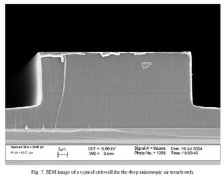
My take as a process engineer is that something has to be done to improve the litho pattern transfer, and I suspect it might be EUV, unless this pic of the ram cell is already patterned with EUV litho?

CONT'D - click READ MORE.... for the full scoop.


Or possibly the dry etch nanoscale uniformity / roughness, which at this nm level can be either the dry etch OR the nano-scale morphology of the gate electrode thin films. All in all, fascinating process detective work opportinuties. I'd love to fix this and to hell with the CAD solution. It is root cause a process issue.

MY guess this is keeping many folks up at nite to figure out some more pragmatic solution for 45nm production with tight parametric control needed for predictable circuit design performance.

POSTSCRIPT Feb 15th 2006 - the other interesting aspect to this, is that the image posted by Intel of the 45nm SRAM cell, is a SEM [Scanning Electron Microscope] image. Despite the hullabaloo about AFM metrology, when SEM electron microscope instrumentation is up to snuff, and well designed, no AFM can come close to the speed, accuracy and calibration stability comparable to that acheivable with the best electron optics imaging. It is quite telling that Dr. Mike Kirk, formerly a senior scientist at Park Scientific, is nowVP of the high end imaging & metrology business line at KLA-Tencor, per a recent EE Times news release about the latest SEM metrology tool being fielded at the firm.


Article on the genesis of Adherex Technology - novel safe cancer pharmaceuticals

Prof. Orest Blaschuk, McGill University
founder of Adherex and a most prolific inventor


Originally from the Ottawa Citizen, by James Bagnall, this superb article describes the early days of Adherex, its merger with Oxiquant and moreover a succinct description of why Cadherin antagonists have such astounding promise as cancer pharmaceuticals - safely destroying a useful % of a targeted class of solid tumors, with few to no side effects, nor any toxicity observed in phase 1 FDA (where a large tumor was apparently completely destroyed). on AMEX on TSX

POSTSCRIPT March 9th 2007 - since the early 2006 posting of this blog article, ADH-1 has been found to be largely complementary to conventional chemos - where conventional chemos seem to attack mostly e-cadherin tumor tissue, conventional chemos seem largely to not treat / destroy n-cadherin marked tumor tissue that ADH-1 seems to target so effectively.

While ADH-1 is almost perfectly safe (natural human metabolic pathway, from its basic human natural source) ADH-1 will likely find its home in combo therapy with conventional chemos that target specific tumors and will likely it seems change prognoses quite markedly for the better in quite a few tumor types. (based on early preliminary non clinical tests described in Adherex public conference calls)

ALSO the expertise of Dr. Peters and Norris is evidently profound - with Adherex's apparent quick technical fix to Glaxo's misfire on Glaxo's ~$80m development of 5FU/Eniluracil, Peters and his team have demonstrated in a mouse model the proper ratios of 5FU to Eniluracil fix most all the problems Glaxo saw and Adherex did this in ALL OF 3-4 months to mouse data reported!!

Adherex's 5FU/Eniluracil program will likely be an excellent PATENTABLE advance in orally administered "conventional" chemotherapy.

MY compliments to the superb ADHEREX TEAM !!

I will also point out that i HATE hollow investments touted as innovative and implied as successful in commercial mileu. REAL innovation is by dint of observation of careful methodical experiment and in Biotech is often NOT the result of expensive COMBINATORIAL
shotgun experiments - by inexperienced wannabees. Careful scientific advances of commercial import come from keen observation and relevant skills - beating the well monied time and time again.

Another notable advance looming is in possible reversing of Diabetes by a team at Sick Kids Hospital in Toronto with pedigree in research dating back to the discovery of insulin. ALL DONE ON A SHOESTRING BUDGET, just like Orest was largely underfunded, the Toronto advance was done with a simple experiment first killing excess neurons in the pancreas with pepper extract capsaicin, and then injecting a neuropeptide to kick insulin regulation back into operation, tested for 4 months revival. So far
just done with a mouse model, but with potentially huge implications for a possible real cure to diabetes. INNOVATIONS by real experts rather than "purported advances" by wannabees as is more common with Biotech.

Here is the news release from the hospital that did the actual early novel diabetes studies - Sick Kids Hospital in Toronto

http://www.sickkids.ca/mediaroom/custom/diabetesopen06.asp

The key researchers - some profiles

http://www.sickkids.ca/HSCdirectory/personalprofile.asp?pID=2345&sID=1104&s=Research+Programs&ssID=378&ss=Neurosciences+%26+Mental+Health


http://www.canadianpaincoalition.ca/index.php/en/about-us/board-of-directors/micheal-salter


I will also remark that there are hints that MS might be treatable by comparable means - where capsaicin might be able to change outcomes of MS, but this is mere speculation on my part ( ie possibly by killing defective nerves and stimulating healthy regrowth? or limiting further degradation, although the means for effective targeted delivery to specific sites of early damage is not a minor problem technically, but one might hypothesize that MS was initially localized neurological damage that if caught early could in fact be treated before spreading significantly by eliminating the damaged regions.??? I have to explore
this a bit more to come down from the wild ass stratosphere .... )

[ Aug 19th 2007, I happened to stumble on a goldmine re MS understanding. In short MS seems to be associated with a type of viral infection, in early stage of the understanding. Here are some relevant web sites - 2 blogs and the research group site of a leading researcher in this area of understanding Multiple Sclerosis :

hervs-and-multiple-sclerosis-part-1
hervs-and-multiple-sclerosis-part-2
some background on endogenous retroviruses
endogenous-retroviruses-and-evidence

and a researcher leading the way to the understanding correlation between a viral infection and multiple sclerosis (ie that a specific viral infection causes Multiple Sclerosis ) - Prof. Christopher Power MD, at the University of Alberta Department of Neurology... brainpowerlab ]

And yes I like identifying real innovations.... outperform the speculators and pumpers, with real advances analysed and followed closely. That is investing.

I am happy to help any and all in doing due diligence on any prospective tech or bio investment. Contact me through comments for further discussions (I will not publish your inquiries)

Monday, February 13, 2006

Finally SWNT ( single wall carbon nanotube ) Forests might find a novel performance application


Prof Joel Schindall leads the way.

The application & performance seems promising, and not semingly daunting to build, yet leverages the ease of high surface area to volume for nanotubes seemingly quite simply.

Are there any issues in the device structure fab, outside of the SWNT nanotube forest growth
which is pretty well understood.

Can this be made cheaply enough to find a nice market of decent volume and profits?

When will real devices make it out ?

Sunday, February 12, 2006

MSN SEARCH - it Indexes Blogs Nicely .....

Saturday, February 11, 2006

Another Puzzle - this time Thin Films Related

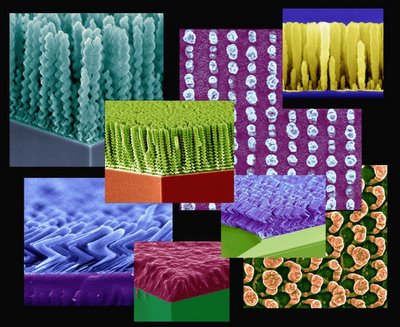
Glancing Angle Deposition (GLAD)

Colorized SEM collage with permission of Prof. Michael Brett University of Alberta
Description & pics below with permission of Prof. Kevin Robbie Queens University

CONT'D - click READ MORE.... for the full scoop.

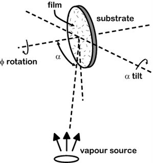
Glancing Angle Deposition (GLAD) is a technique for fabricating materials with controlled structure. It is based on thin film deposition, by evaporation or sputtering, and employs oblique angle deposition flux and substrate motion to allow nanometer scale control of structure in engineered materials.
The substrate is oriented at a large oblique angle relative to the incident vapour flux (a > 75). This leads to an effect called atomic shadowing and results in a porous structure with isolated columns of material growing toward the vapour source. The substrate is then rotated or tilted during deposition to engineer desired microstructures.


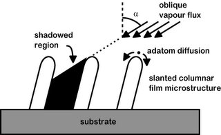
Atomic shadowing occurs when oblique vapour flux is shadowed by previously deposited film material from reaching areas on the substrate. These areas are shadowed. If the mobility of the atoms on the surface (adatoms) is limited, there is no growth in the shadowed regions. This results in the porous inclined microstructure observed in oblique deposition.


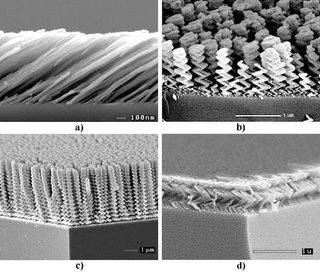
This figure shows the fundamental techniques used in GLAD with MgF2 films deposited on Si or glass. All 4 films were deposited with the polar flux angle a equal to about 85 degrees. In a), the substrate was held stationary and the flux arrived from the right for the entire deposition. A porous inclined microstructure resulted. In b), the direction of arrival of the flux was alternated from the left and right 12 times during deposition. Note that the polar angle a was kept fixed at 85 degrees for the entire deposition. In c), the substrate was rotated continuously during deposition. The film growth was always toward the vapour source so this resulted in a helical structure. A feedback control system was used to adjust rotation rate to accommodate for varying deposition rate and achieve constant pitch helices. In d), a combination of the techniques used in b) and c) was used. The substrate was rotated in 90 degree steps during deposition. A short pause for deposition followed each 90 degree rotation and the resulting structure is a 4 sided 'square helix'.


Effective Yield Improvement in Semiconductor Manufacturing

Good Habits for Yield Improvement Engineering
List in no Particular Priority
( ie this is NOT your Mother's Yield Solutions Overkill )

1] GATHER INFO - Anecdotes, Data, listen to opinions[every last one till you are bored 5x over, even from the 2nd shift operator], observe and dig, till your fingernails are ragged bare.

2] MAKE NO JUDGEMENTS YET - be a good, even great listener

3] Do not hew to unsubstantiated preconceived ideas YET, no matter who says it ( same as 2])

4] MAKE LISTS ( bigger the better & then prioritize ) - some call 'em Fishbone.

The former Director of Hitachi Central R&D labs, kept his low yield hypothesis list, on a single 3x5 unlined index card - as a dense list of brainstorms and corresponding hoped for tests of validity. Fishbone diagrams per se, are often merely tools for the inexperienced, and those too stiff to really brainstorm enjoyably.

It is the list writing and reflections thereupon continually - that matters and something of character - leave no stone unturned, as you never know what the cause is, until proven by a working process FIX.

I'd make the same case for over obsessing about Xbar R, process trend charts - the most important thing is to use them, not obsess about the numbers, but to look at the trend data continually and skeptically as to "your process' stability", and check potential root causes. Xbar R is a window into the soul of your processes and read it carefully.

5] View everything with a healthy dose of skepticism, not cynically, but ANALYTICALLY.

My best Fab Wide yield fix (+20% increase, to return a showcase bleeding tech - crashing fab to "normal yield") occurred in spite of "substantiating" data indicating the REAL SOURCE of yield loss - was "purportedly guilt free".

EVEN numerically correct experiment analyses, can lead to making WRONG conclusions.

A T-Test "proved" innocence, BUT a MINOR REALITY CHECK INTRUDED - the experiment design did not account for a critical process integration matter which rendered the T-Test results INVALID as interpreted.

TRUST BUT VERIFY, not to be mean to others, but to UNDERSTAND the experiment, data and purported conclusions.

EVERYTHING HAS CONTEXT, and context has bounds or limits to interpretation.

6] DO LITERATURE SEARCHES when you are in need of fresh ideas - not some trite 1 marquee article and call it a day. READ dammit.

7] CALL VENDOR APPLICATIONS EXPERT"S", and drill down through organizations until you get what you really need, not to feebly fob it off as "the sales guy did not know".

Expert knowledge comes from experts, and the best help is often free, if you take the time to actually persue it with sufficient vigor.

And to really mess with you mind, once you have the expert opinion, sometimes do the opposite (not exclusively) since this might merely be conventional wisdom of an expert, but listen carefully just the same.

8] Mull all this data over, think, pick your best shot from your list of hypotheses, and run experiment (s) testing your hypothesis' validity.
Pass - collect the accolades.
Fail, go to the next best candidate on your working list.
Repeat as necesssary until you find the real solution, or give up prematurely, stumped in your quest ( hopefully it does not come to this ).

9] CHARACTER MATTERS, try your darndest, and search after real root causes with persistence and dogged determination.

Be your own best critic, not to be despondent when things don't work out as hoped for, but to be true to yourself first.

My own motto when faced with the seemingly daunting insurmountable task was "you can't hit a home run unless you first swing the bat" ( and I have plenty of strikeouts under my belt).

Don't pay attention to others' misconceptions, and browbeating, nor nitpicking, focus on the task at hand, like a horse with blinders on.

Swing the bat regularly with good intentions, and you will develop great problem solving skills (harder than R&D / inventing BTW)


and finally .....
10] NEVER GET YOUR CUSTOMERS DRUNK, to convince them to pay their bills.

One yield consultancy - quite prestigous, in the course of an interview, I asked - "How often do fab yield improvement customers not choose to pay?" and the response was "pretty frequently that they fail to belly up and pay their debts..."

So I then asked - "how do you get your customers to pay up when they refuse?" and the youthful hiring manager responded "I take the customers' managers out to dinner and gets them plastered enough to sign on the dotted line of their contract, while thoroughly soused".

Sad, and not quite ethical, despite the pedigree of the well known firm.


Thursday, February 09, 2006

Who is this Sage Giant Among VC Advisors to Startups ?


and what are two ( among several ) prominent career milestones he acheived prior to calling silicon valley home, nevermind his near continual string of blockbuster startup hits ( and being universally well liked and immensely respected )?

END OF POST.....

What Role in the Dawning of a New Age of Science


do these two pictures relate to -
Who is she and
What precisely transpired that was significant and not given due recognition until much later?


END OF POST .........

Late 1950's MACH 2 Interceptor on the Tarmac

WHAT AIRCRAFT IS THIS?

END OF POST .....

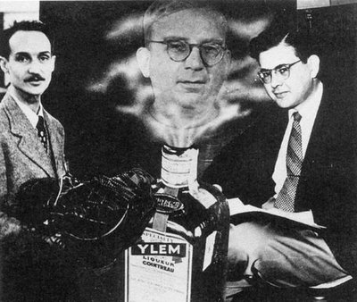
What Echos of Cointreau is this YLEM ?


and what did it mean to the understanding of the universe?
( note to SJ - these pictoral puzzles are following in your fine FLIKR tradition except highly nano-ist in orientation )

END OF POST ...............

Who Is This ?


Some might call him "Nemesis of Sand Hill Road"? and a very successful one at that - the distinguished Rider, who happens to be a very successful inventor, scientist and businessman.

The Horse, silly, is merely lucky, (ed. correction "was", as the Horse recently passed on) with his stable not far from the former Reagan ranch, on one of the larger spreads in the region ...

Wednesday, February 08, 2006

TETRAD of PhotoVoltaic Materials Strategies for the future

Things to Ponder

SILICON - variations on process & module methodology
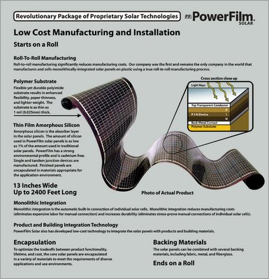
single xtal, thin film and poly xtal, hot wire cvd and small chips, Prof. Sach's edge fed string growth, emerging/ speculative silicon nanowire and the superb engineering of Sunpower's sophisticated devices......and now a large scale 13" wide - roll to roll amorphous silicon on polymide flex at Iowa Thin Film Technologies AKA Powerfilm Solar

the cast of millions goes on and on...

CONT'D - click READ MORE.... for the full scoop.
POLYMER Photovoltaics -
Konarka
The best top flight VCs are betting on this.
The most prestigous board and advisory team.
1] founding scientists
2] industry advisors
3] science advisors
Based on names alone it will likely succeed.

And very notably, Prof. Heegers superbly prolific patenting is beyond merely impressive, an astounding personal ~60 career patents.

Kudos to Prof. Heeger !

Will a means be found to inhibit UV / environmental degradation needed for a competitive product life ?

Will it be possible to coax stable and usefully high PV efficiency from some as unknown EVIDENT materials solution? ( silly pun of mine )

Feb 14th Konarka announces another $20m funding round completed lead by 3i ventures, making a total $60m raised since 2001.

Stay Tuned .... ( again a silly pun only a photon would love ? )

NANOCRYSTAL PV conversion
Nanosys - seems to still be struggling with %PV conversion efficiency
as Konarka seems to be ?
Are tetrapods all they are cracked up to be?

Cyrium Technologies - Fafard's Nanoscale Self Assembled EPI Quantum Dot solar cells
Simon F. says he can hit in excess of 40% conversion efficiciency for space based cells, the real question is whether he will get bit by the bug for larger price sensitive markets and try to put some effort into a scalable production worthy terrestrial oriented PV device based on SA Quantum Epi Dots. Fafard is CNRCs quantum dot expert, and spent time in a post doc at UCSB under the ever fascinating and mercurial Pierre Petroff.

Cyrium does need to increase the size of the patent portfolio that is certain, as the firm is nowhere near the # of filings of larger competitors, but likely is that Cyrium's present funding is a notable constraint. Simon's core IP is represented in "Solar cell with epitaxially grown quantum dot material" United States Application 20050155641, which describes successively cascaded tuned QD PV elements merely grown epitaxially.

For now that is all that is apparent in the relevant IP posted at USPTO. If it makes it to an issued patent, this might be of considerable value, beyond the bond layer transfer tandem cells being studied at Caltech and elsewhere, merely on ease of manufacture, by avoiding the multiple bond layer transfer of this earlier innovation practiced at the Atwater Lab.

Technically at some point, the self evident paradigm to try, is to leverage the methods fairly recently implemented at Motorola for III-V low defect EPI growth on large silicon wafers, for his devices.

Question is whether Cyrium has motivation, interest or knowledge for how to do so. If yes to all 3, and one can acheive comparably high efficiencies on larger wafers from "mere" epi growth, question is, will this catalyze a larger terrestrial market and higher profits, when competing against for example SunPower's lean mean manufacturing machine? "Only a photon knows for sure ..."

Thin Film CIGS
Miasole
Promising but capital intensive ( almost unnecessarily so with the advanced custom magnetron sputtering cathode that was entirely unnecessary to be part of the complex critical path in the production process development - despite the appeal of high utilization cathodes, where was it impotant in determining the actual panel / module process flow - NOWHERE ??? and costly thin stainless substrates.

And it is likely that they made 2 Process strategy ERRORS. The stainless flex substrates have a host of implied problems - mostly related to singulation and possible edge shorting of the cell structure during singulation, not to mention adhesion / CTE mismatch issues in the thermal cycling for CIGS interdiffusion activation.

The described method of shear cutting the edge of the web steel, while it looks clean in cartoon pics, is risking serious damage to the junction integrity of the CIGs stack, unless a laser preclean is done to remove the CIGS stack from proximity to the sheared edge - but with still yet the remaining risk of shear induced cracking of CIGS in proximity to even a cleaned edge of the stainless substrate.

Furthermore laser processing of materials on top of stainless flex substrate is going to make the laser process window considerably smaller than desired due to high power losses to the steel (heat sinking), which is completely undesireable for a good industrial (yag) laser ablation process. And yes athermal fast excimer pulses will help, but at much greater cost than typical industrial grade YAG laser thermalized processing. And if you still yet need more process window - the trick will be to reduce the laser power required with reactive gas assist laser etching rather than purely ablation, while it may make a useful process window, will result in consdierably higher capital costs, nevermind some risk to the CIGS itself. So high thermal conductivity ( steel) substrates for web fed CIGS are coming with some considerable baggage technically.

Therefore, while steel has an obvious ( to those who have workd with laser ablation process ) serious set of disadvantages in process integration, the potential aesthetic and relaibility appeal is quickly lost in practice.

The means to slightly shift things in ones favor, is to carefully examine process windows and adapt materials to


and naturally in module integration is the ever present, tantalizing yet slightly fickle ....

Roll To Roll Processing
Nanosolar ( PV ink ) as a Paradigm for cost reduction for module formation and further mention to the "ROLL MASTERS" large scale 13" wide - roll to roll amorphous silicon on polymide flex at Iowa Thin Film Technologies AKA Powerfilm Solar


Roll to Roll has unique materials and structure requirements to acheive long life cells, and forces the manufacturer to look closely to find capable production equipment for end to end Roll to Roll.

RtoR sputtering is easy to procure std equipment for, but patterning / ? screen printing takes a bit more effort ) [ come to think of it - screen printing or resist litho & etch in RtoR, is almost silly - just go with Shadow Masked metal sputtering for the coarse PV interconnect features - with no need to etch, nor fire a screen printed paste ]

and more speculatively - will the Vitex Barix process find a home in environmental barriers in some of the more novel PV advances ( as it has been successful in OLED stabilization without the use of hermetic sealed packages ). This is something only an OLED pioneer might know?

musings to follow later .......


Enter your email address:

Delivered by FeedBurner

Subscribe to Wendmans Views on Nanotech by Email